This thread has been locked.

If you have a related question, please click the "Ask a related question" button in the top right corner. The newly created question will be automatically linked to this question.

CDCLVP1216: How to process Vac_ref pin if I don't use it?

Part Number: CDCLVP1216
Other Parts Discussed in Thread: CDCLVP1204

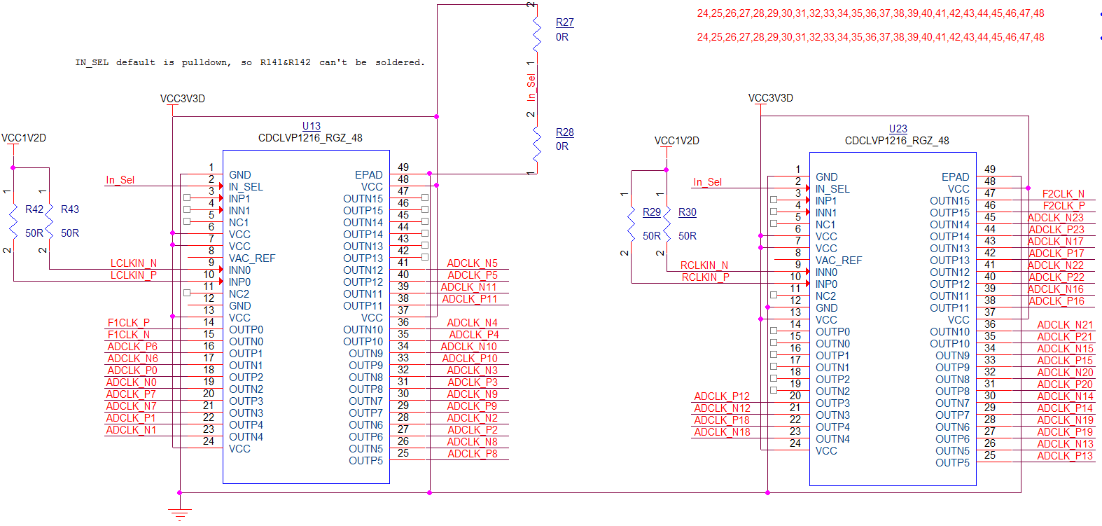
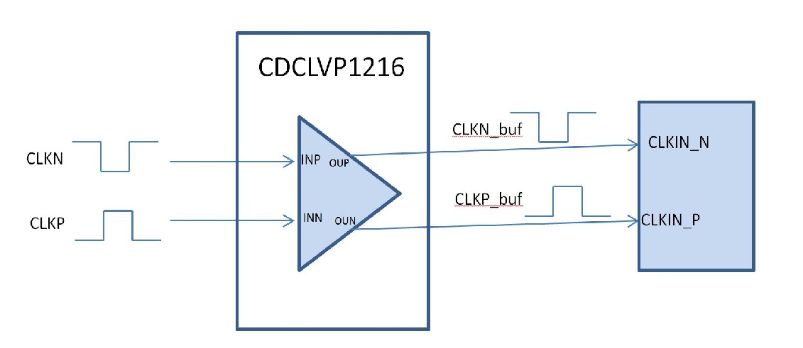
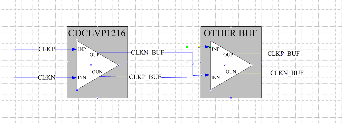
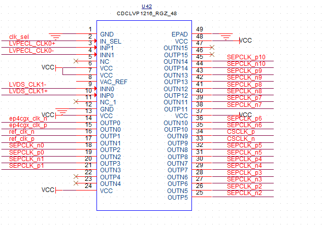
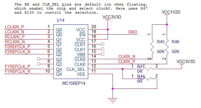
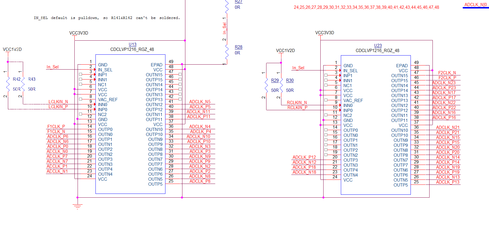
We are using CDCLVP1216 to replace ON-Semi's NB100LVEP224. We used board provided 1.2V to pull-up 50 ohm on each input leg to couple LVPECL clock when we used NB100LVEP224. Now we want to use same method on CDClvp1216, however, how to process pin Vac_ref, can we leave it float? I attach our schematic design here, please help us checking with it.

Thanks

  • Hi Won

    You can leave the Vac_ref pin floating if not used.

    Best regards
    Puneet
  • Hello Puneet,

    Thanks for you reply.

    I have another question need you help. In order to make it easy for PCB routable, can i swap the differential clock's n leg with p leg? I am talking about both input and output channels.

    Best regard

  • Hi Won,

    Yes you can do that.

    Regards
    Puneet
  • Hi Puneet,

    You mean i can do that ignore the front and next end of the CDCLVP1216? You know, the CDCLVP1216 outputs destination include other clock buffers, or FPGA clock input, or ADC input clock. It means CDCLVP1216's out*_n will be connected to other clock buffer input's (or FPGA, or ADC) clkin_p, and out*_p will be connected to clkin_n, can i still do like this?
  • Hi Won,

    I am not sure if i understood your concern right, please have a look at the attached drawing. there should be no issue this way.

    Best regards

    Puneet

  • Hi Puneet,

    Your drawing is one of my schemes. Actually, the first stage, CDCLVP1216's input is connected nromally. We just swap CDCLVP1216's output channels. I also draw one picture to show it.

    I try to describe how we use CDCLVP1216 in our system in detail. Above picture is the simple block diagram. The clock soure for our system is coming from our backplane board. One piece CDCLVP1216 is used on backplane board to distribute about 14 channels clock outputs for other sub-boards and FPGA on backplane. The schematic design as below:

    You can see that  all of above CDCLVP1216's output channels are swapped. The sub-board's clock circuit is design as below:

    The CLKIN_N&CLKIN_P of MC100EP14 are from above CDCLVP1216 outputs (CLKIN_N=SEPCLK_n). Can i say the clocks are only inverted(or 180 degree shifted)?

    Then the MC100EP14 drives two pices CDCLVP1216  and two FPGA clock input normally, as below picture shows:

    BTW,do i need to check the common mode voltage between CDCLVP1216 and MC100EP14? Otherwise, i should make AC couple between them?

  • Hi Won,

    Yes you are right, as you have swapped the Clock P/N in the clock path one time, you have inverted the clocks.

    You will have to take care about the common mode at the interface between CDC & MC devices. It should be within the datasheet limits.

    Why are you using MC100? CDCLVP1204 should work as well!

    Best regards
    Puneet
  • Hi Puneet,

    If there are several stages clock buffers (like our application), is it means that i can swap clock pairs at any points, and swap any times? And if do like that will affect clock signal quality?

    Our previous system used NB100LVP224+MC100ep14, now we convert to cdclvp1216. Actually, i planned to replace mc100ep14 by lmk00725pwr without changing circuit design. However, it's not possible after check both mc100ep14 and lmk00725pwr 's datasheet. Though footprint of these two parts are same, one or two pins definition are different.
  • Hi Won,

    Yes, from clock buffers point of view, you can swap the clocks at any time. There is no clock quality difference.

    Best regards
    Puneet