This thread has been locked.

If you have a related question, please click the "Ask a related question" button in the top right corner. The newly created question will be automatically linked to this question.

CDCE62005

Other Parts Discussed in Thread: CDCE62005

Hi :

Need kind help on CDCE62005 design.

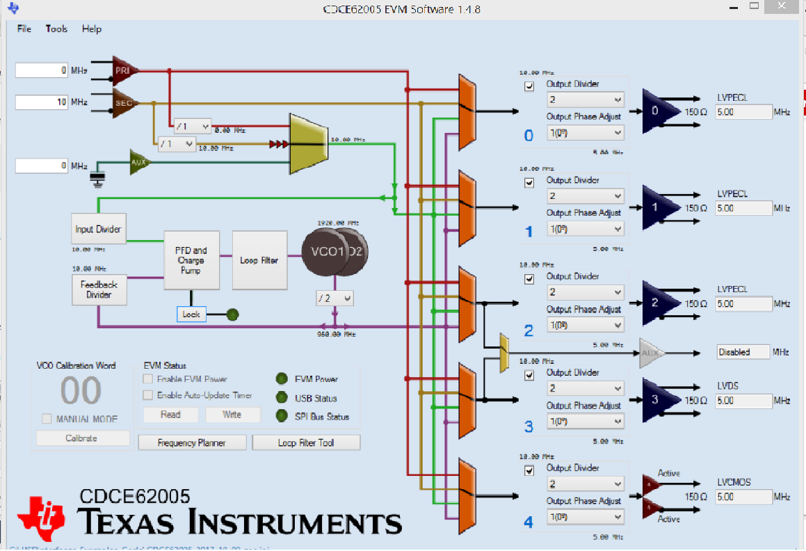
I use 10MHz reference clock for PRI_REF and SEC_REF,  and use VC++ Interface code to set up registers, I tried many register configurations, one of the register setting is as below:

Reg_0 0xEB840000
Reg_1 0xEB840021
Reg_2 0xEB860302
Reg_3 0xEB860303
Reg_4 0xEB860334
Reg_5 0x800C6E45
Reg_6 0x84BE19C6
Reg_7 0xFD90FBA7

Reg_8 0x200099F8

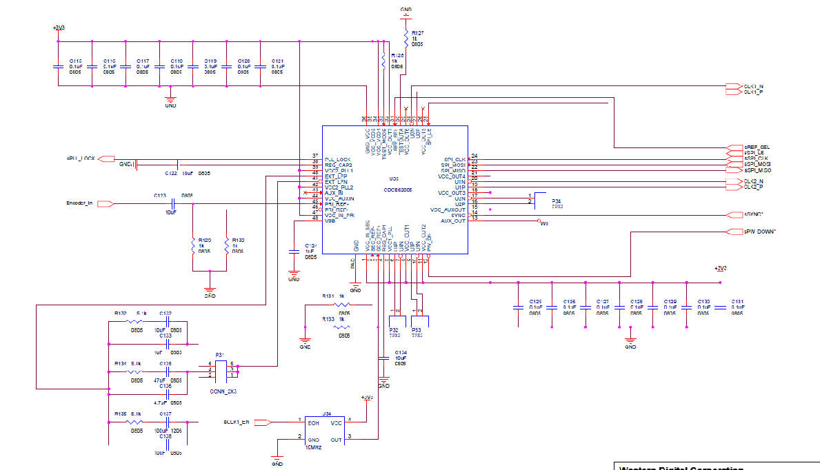
After writing these registers, I can read back the same setting through sSPI_MISO on all registers, which tells me SPI interface is working. 

The purpose of the design is to see two output clocks on U0 and U1 generated from PRI_REF input. But, I couldn't see clock signals on any output ports.

I don't know if it's hardware problem or not.  Can anyone help me check the setting or give any suggestions?

Thank you very much in advance!

  • Hi Li Zou,
    Try to use CDCE62005 GUI to generate register values.
    www.ti.com/.../scac105

    Please double check 10 MHz input type (LVCMOS, LVEPCL, LVDS).
    What's your output clocks frequency and type?

    If the problem had not been solve, please upload schematic for TI checking.

    Regards,
    Shawn
  • Hi Shawn,

    Thanks for your kind help. 

    There's only SEC_REF input (10 MHz, LVCMOS) used in my design, and directly passed to all output channels.

    The ini file generated from above GUI, and used in my design:

    REGISTERS
    0 81800220
    1 81800221
    2 81800202
    3 EB800203
    4 01800214
    5 10000E85
    6 040E0B66
    7 BD0037F7
    8 20009D98

    PORTS
    0 9D
    1 FF
    2 DF
    3 F9

    INPUTS
    PRI 0
    SEC 10
    AUX 0

    EXTERNAL COMPONENTS
    C4 1
    R4 1
    C5 1

    The schematic I am using is as below:

    All registers are working properly with writing and reading, but,  I couldn't detect any output clock signals. Is there anything wrong with the circuit design?

    I really appreciate your help!

    Li

  • Hi Li,
    The register values looks well in GUI.

    The schematic capture is not clear. Please check below items.
    1, Make sure each Vcc pin get correct 3.3V.
    2, In case of LVCMOS input on SEC_REF+, connect pin SEC_REF- through 1 kΩ resistor to GND.
    3, Make sure LVPECL output need a DC bias resistor 150 Ohm to GND on each line.
    4, Make sure LVDS output has an 100 Ohm load.

    Hope helpful for you.

    regards,
    Shawn
  • Hi Shawn,

    Checked and modified our design per your suggestion, VCC and GND pins connect correctly, and ouput pins add a DC bias resistor 150 ohm to GND. 

    If CDCE62005 EVM Board powered up, there are 1.6V on YN pins and 2.5V on YP pins, but, all YN and YP pins in my design have no DC voltage detected after powered up. In my design, VCC pins connect to 3.3 V power, and registers have no problem with write and read process. 

    May I know whether we need to check the Thermal_PAD connection, or need to replace the CDCE62005 chip, or have to use the differential inputs (LVPECL, LVDS) for PRI_REF / SEC_REF? 

    Thanks you very much,

    Li

  • Hi Li,

    Please check voltage on pins 12 /Power_Down & pin 14 /SYNC. They should be kept in HIGH for normal operation.

    More output OFF statuses could be found in table 15 in CDCE62005 datasheet.

    Regards,

    Shawn

  • Hi Shawn,

    My system works after setting the pin 14 /SYNC to high in the interface code.

    Thank you so much for all the help.

    Li