A related question is a question created from another question. When the related question is created, it will be automatically linked to the original question.
If you have a related question, please click the "Ask a related question" button in the top right corner. The newly created question will be automatically linked to this question.
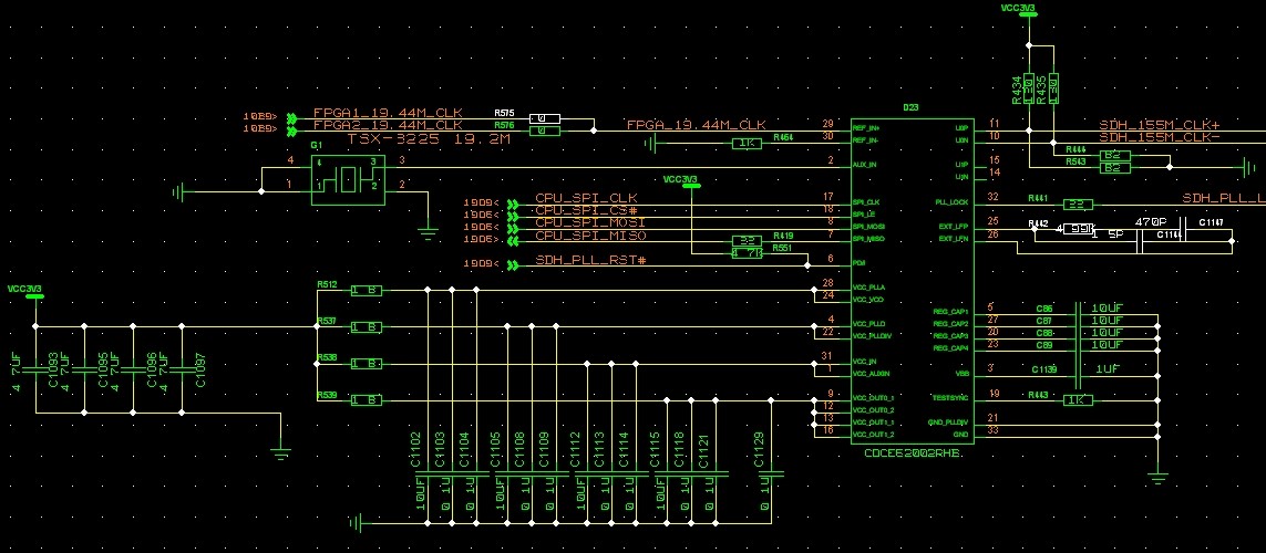
CDCE62002: What need pay attention about design? And PCB design?
Place a 0.1uF bypass capacitor on each VCC_OUTx pin
It is recommended to move the termination resistors (R434, R435, R543, R444) from the input to the receiver. In the schematic the resistors are placed by the output of CDCE62005
For the crystal, it needs to have a load capacitance of 8-10pF and ESR below 50 ohms, placed close to the CDCE62002. If the load capacitance is less than 10pF, add a parallel load capacitor to match the on-chip load capacitance. For best performance, you may decide to include a PCB cutout region below the crystal to prevent interference for better performance.
For PCB design, it is important to route the output traces as a 50-ohm controlled impedance differential pair to get best performance. In general, place bypass capacitors as close to the device as possible. Other than that, this app note highlights layout considerations for high speed signals: www.ti.com/.../scaa082a.pdf
Many thanks for your advise, and customer has other issue about the case:
There will happen that can not lock AUX_in, at this time, only use AUX_in signal, REF_in signal does not output any signal.
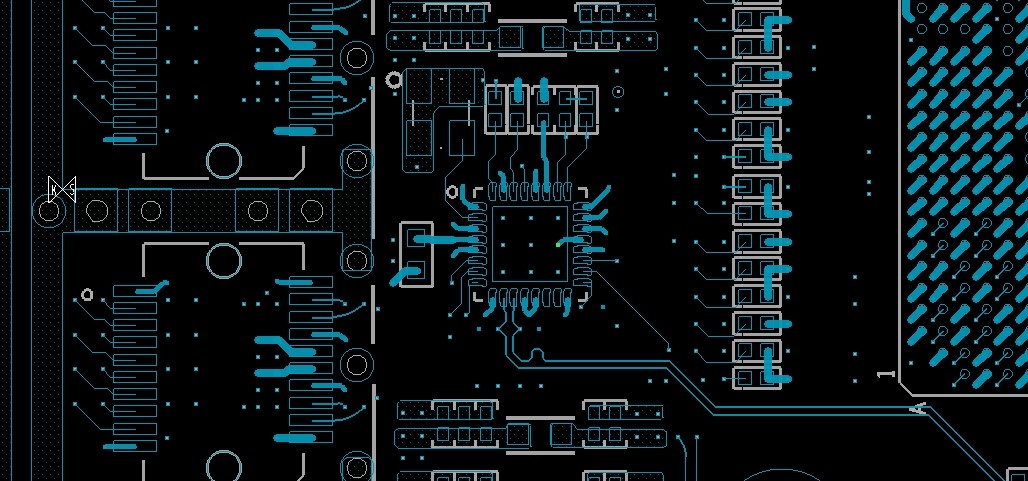
As long as it can be locked, the output is no problem, but often can not be locked, I do not know what will be related to! At present, the crystal load we use is 10pf, the crystal is very close to the chip. We tried to change the load capacitance to 20pf, +-20ppm crystal. This crystal is directly inserted, directly soldered to the two of the surface mount capacitors. The tube is on the line, but the crystal is super high, and the current feeling is not related to the description of the data. I don't know what the specific reason is! Pcb is as follows, the crystal output to the chip input is 196mil, is this route suitable? Impedance single-ended 50Ω.
Are you having the same issues when using REF_in? The XTAL placement looks OK. Is the ESR of the crystal less than 50 ohms? What is the drive level of your crystal? You may need to recalibrate the VCO in order to lock the PLL. You can manually recalibrate the VCO according to datasheet section 9.3.8 . Also, make sure the the reference selection mux is properly configured. You can set R0[2:3] = 0b01 for AUX, or R0[2:3] = 0b11 for Auto-select. See datasheet section 9.3.5.2 for more information. I hope this helps!