Hi team,
Below is the schematic of the CDCLVC1310.

But customer test the XIN pin and get below wave:
Can you help to comment what's the cause of the issue?
is it because the cap input value or maybe the PCB layout?
Lacey
Thanks a lot!
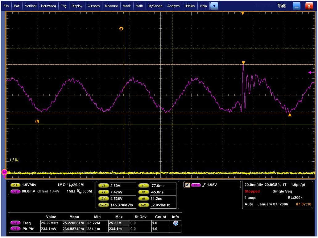
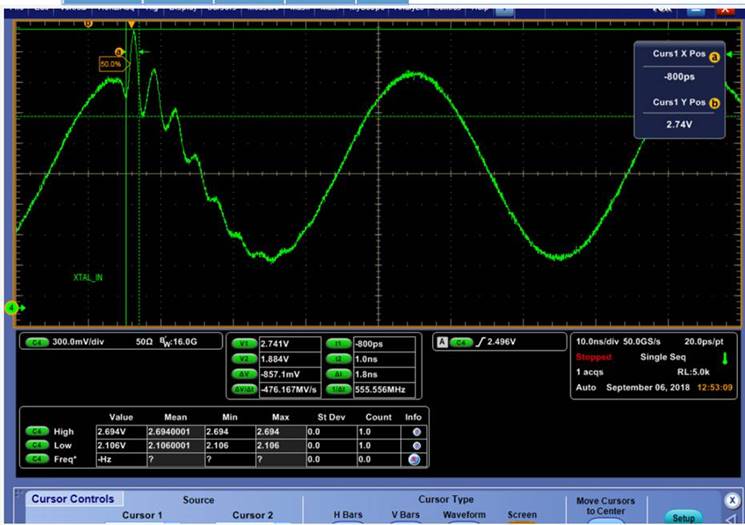
Hi team,
Below is the schematic of the CDCLVC1310.
But customer test the XIN pin and get below wave:
Can you help to comment what's the cause of the issue?
is it because the cap input value or maybe the PCB layout?
Lacey
Thanks a lot!