- How does the PWM example in the data sheet work?
- What are the limitations of the data sheet PWM example?
- Is there a way to improve linearity and duty cycle range?
This thread has been locked.
If you have a related question, please click the "Ask a related question" button in the top right corner. The newly created question will be automatically linked to this question.
This FAQ covers PWM circuits. Figure 1 below shows a pulse width modulator using the LM555, NA555, NE555, SA555 and SE555 timers that are called LM, NA, NE, SA and SE respectively hereafter. As a group they are called bipolar timers due to their design. This FAQ also covers LMC555 and TLC555 timers that will be called LMC and TLC respectively hereafter. As a group they are called CMOS timers due to their design. This FAQ is applicable to the xx556, TLC551, and TLC552 timers as well. Supply voltage pins for the timers use different symbols, namely VS, VCC, and VDD, that have the same function.
Data sheet example circuit
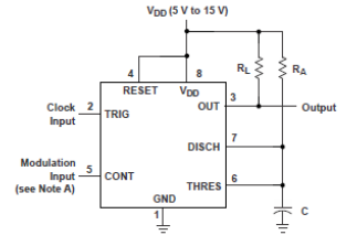
The data sheets show this setup to implement a PWM using a 555 timer:
Figure 1. Data sheet example (pin 2 is input clock, FI)
The circuit in Figure 1 is a mono-stable pulse generator that provides an output high time that is ideally –RA*C*ln(1-VCONT/VDD). The output frequency will ideally match the clock input frequency, FI. The resulting output duty cycle is –RA*C*ln(1-VCONT/VDD)/FI. Therefore the output duty cycle varies with VCONT in a non-linear fashion. The nonlinearity is a result of the timing capacitor ramp being an exponential curve. Duty cycle also varies with RA, C and FI.
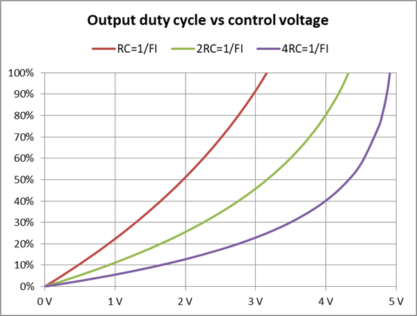
The data sheet example uses values of RA = 3kΩ and C = 20nF, which sets the RC time constant value, RA*C, to 60µs. The example mentions that the RA*C product is set to the clock period divided by four. In other words, the 240µs period is 4 times the RA*C product. The control voltage to duty cycle transfer function for this setup can be seen in the 4RC = 1/FI plot in figure 2. Clearly, the linearity is very poor. The results for RA*C values that are closer to the input clock period, such as RC =1/FI and 2RC =1/FI, are more linear. Note that increasing the RC product also compresses the control voltage range. Figure 2 represents the ideal transfer function for different RC time constants relative to input clock period.
Figure 2. Duty cycle vs control voltage for various R*C products per timing period, 1/FI. VDD=5V
When designing a PWM signal with a 555 timer, there are additional limiting factors to consider. For example, the external clock driving the trigger input must have a low negative duty cycle, output low time percentage, because the PWM output minimum high time cannot be less than the input clock low time. The external clock can be generated with another 555 timer in an a-stable setup. Operation below 10% or near 100% duty cycle can cause extra or missing output pulses. In the latter case, duty cycle and output frequency drops in half. The minimum useful control voltage for LMC is 0.4V and the TLC minimum is 0.5V. Operation at lower control voltages will result in a duty cycle that is fixed or may cause an inconsistent pulse stream.
The bipolar timers have a storage delay of about 16µs which can limit the minimum duty cycle. The maximum duty cycle for these devices is limited to about 97%. Adjusting the control voltage to attempt a higher duty cycle will create an output that has frequency division. In such cases, the frequency is divided because there are missing output low pulses, resulting in a duty cycle near 50%. The bipolar timers also have increased threshold current when input voltage is close to VDD. This input bias current can limit the high duty cycle maximum. Adding RL can improve the VOH level for the bipolar timers, but it is not required for any of them.
Using the data sheet example of RA = 3k and C = 20nF with clock periods of 60µs, 120µs, 240µs results in the minimum duty cycles in table 1 and maximum duty cycles in table 2.
Period |
NA |
SE |
LM |
LMC |
TLC |
60µs |
26 % |
25 % |
24 % |
12 % |
16 % |
120µs |
13 % |
14 % |
12 % |
6 % |
8 % |
240µs |
7 % |
7 % |
6 % |
3 % |
4 % |
Limiter |
16us |
16us |
15us |
0.4V |
0.5V |
Table 1: Minimum duty cycle RA=3k, C=20nF
The minimum duty cycle is limited by the 16µs delay of the bipolar timers and the control voltage minimum of the CMOS timers.
Period |
NA |
SE |
LM |
LMC |
TLC |
60µs |
97 % |
95 % |
98 % |
98 % |
98 % |
120µs |
98 % |
98 % |
98 % |
98 % |
98 % |
240µs |
98 % |
85 % |
95 % |
97 % |
98 % |
Table 2: Minimum duty cycle RA=3k, C=20nF
The maximum duty cycle is limited by the occurrence of pulse skipping and also input current on the bipolar timers.
In summary, the data sheet pulse width modulator example is good for applications that are resistant to poor linearity and do not need to operate near 0% or 100% duty cycles.
Improved example circuit
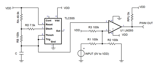
Figure 3 is a much improved, but still imperfect, PWM generator. It uses a 50 percent fixed duty cycle 555 timer oscillator and a comparator. The a-stable oscillator FAQ describes how to make the 50% duty cycle oscillator. Alternatively use these formulas to choose components. RB * C = 0.481 / F, RA = RB / 2, RD = 0.15 * RA, where F is the oscillator frequency. The comparator performs the DC input voltage to output PWM duty cycle conversion. The timing capacitor’s charges and discharges are exponential ramps. However, both the rising and falling ramps are used for the conversion. Therefore, much of the non-linearity is removed. This circuit is useful down to 0% and up to 100% with the condition that the output frequency may be divided. But, the duty cycle will be correct, not 50% as will happen with the figure 1 schematic. R1, R2 and R3 scale the input voltage to between 1/3 to 2/3 VDD to match the timing ramp voltage range. The LM293 needs a VDD of at least 6V to keep the ramp voltage within the input common mode range.
Figure 3. Improved linearity PWM circuit
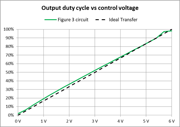
Sample lab results for the figure 3 schematic are presented in figure 4. The dotted line represents an ideal linear transfer function. As can be seen, the output duty cycle of this circuit is more linear than the results from the circuit in figure 1.
Figure 4. PWM duty cycle vs. control voltage using circuit figure 3, VDD = 6V, C = 1nf.
The transfer function result is similar to the ideal transfer function curve.