This thread has been locked.

If you have a related question, please click the "Ask a related question" button in the top right corner. The newly created question will be automatically linked to this question.

LMK04828: LMK04828 & DAC38J84, SYSREF and DAC output timing

Part Number: LMK04828
Other Parts Discussed in Thread: DAC38J84,

Hi team,

We are currently using a Xilinx FPGA Kintex-7 and a Xilinx JESD204 IP core to output analog signals with a TI DAC (DAC38J84).
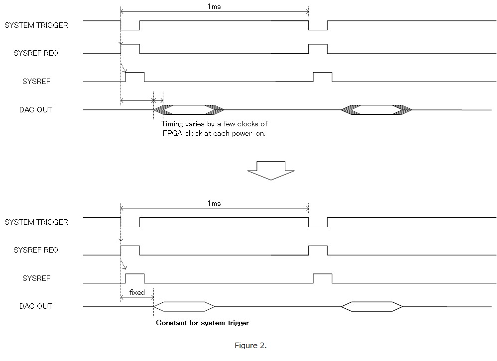
For example, the FPGA receives triggers every 1ms and needs to output an analog signal at that timing, but the analog output timing fluctuates between a few clocks in the FPGA clock every time the power supply is turned on.
However, the analog output timing varies between several clocks at each power supply startup, and we would like to output analog signals at the same timing.
We are using the JESD204B in Subclass 1, but since we do not have much experience with Subclass 1 and do not understand the operation of the JESD204B, we would like to ask you about the following

"Operating Conditions"
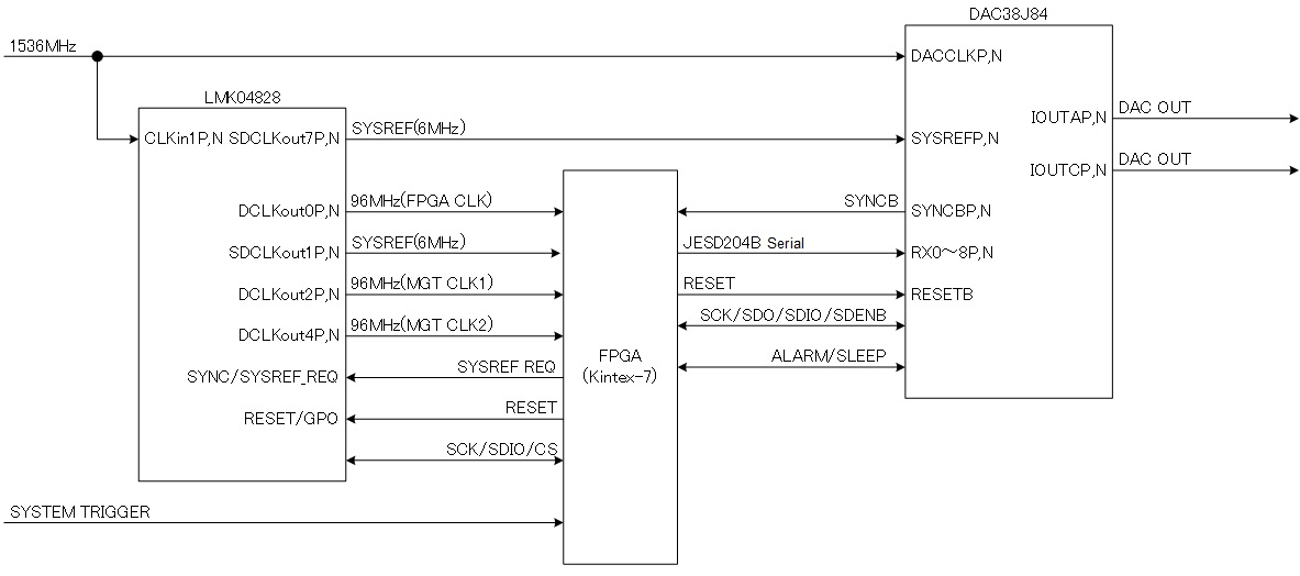
DAC is DAC38J84 and LMK04828 is used for clock and SYSREF generation.
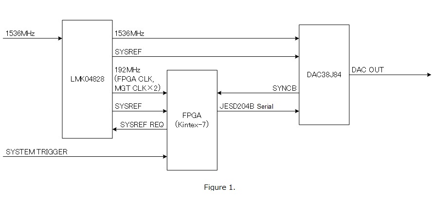
LMK04828 CLKin1/Fin/FBCLKin (pins 34, 35) with 1536MHz input to LMK04828, 1536MHz for DAC, 1536MHz divided by 1536MHz, 192MHz to FPGA and SYSREF (8MHz) to DAC and FPGA (supplied by Pulser to DAC and FPGA). (Figure1)
The FPGA is a Xilinx Kintex-7 with a JESD204 Subclass1 IP core.

"Questions"
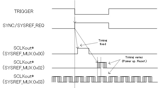
Q1) Is it possible to adjust the phase of SYSREF to the trigger timing that is synchronized with 1ms as shown in the figure2?
In short, I would like to use the trigger as SYSREF_REQ signal and make it the same timing (same delay).
The trigger timing is synchronized with the clock, but the phase relationship with SYSREF changes every time because the timing is different at each startup.
However, since the timing is synchronized with the entire system, the phase relationship is constant after startup. The timing of the trigger and SYSREF does not change.

Q2) I have a question about the operation of the DAC.
For example, if the register is fixed to a certain setting, is the internal delay in the DAC constant or does it fluctuate?
For example, is the internal delay in the DAC for a certain register setting constant, or is there a factor that varies?
It may have something to do with the IP core of the FPGA, but I would like to know if it is possible to output analog signals without any fluctuation in the trigger timing at each startup.

Q3) I have a question about the operation of the DAC.
Is the relationship (delay) between the SYNC signal output from the DAC and the DAC analog signal output constant?
I believe that the timing between FPGA and DAC can only be ascertained by the SYNC signal from the DAC, but I thought that if the relationship between the SYNC and DAC analog signal output is different, it may be difficult to keep the timing constant.

If you have any other points to note (settings, usage, etc.), I would appreciate it if you could give me some advice.


Best regards,

T.Karita

  • Hello,

    My coworker will get back to you tomorrow.

    Regards,
    Hao

  • Hello Karita-san,

    Q1) I can think of two ways to accomplish a constant timing from SYSREF request to analog output timing, as long as the 1ms trigger signal is consistent to within one FPGA clock cycle (the trigger is precise to 1ms ± 2.5ns).

    1. The trigger signal could be used to generate a SYNC pulse, which could be used to precisely reset the phase of the SYSREF divider with respect to the trigger signal. This same technique could also be used to control the output divider phase as well. Although this method is straightforward, it is difficult to precisely reset the SYSREF divider phase without also resetting the device clock divider phase, which means the FPGA clocks could see an interruption - this may not be acceptable for your application. If the SYSREF phase is consistent with respect to FPGA clock phase on each power cycle, you could count the number of FPGA clock cycles between the trigger signal and the SYSREF request, set the SYSREF_DDLY to advance the phase to the right value, and reclock the SYNC signal to the SYSREF divider so that the timing of the divider reset is precise. Reclocking SYNC to the SYSREF divider avoids the problem of resetting the other clock output dividers, but since the SYSREF divider would be reclocking its own reset signal, SYNC_1SHOT_EN should be set to avoid any metastability problems. 
    2. The LMK04828 dynamic delay could be used to advance the phase of the SYSREF clock by an exact number of DAC clock cycles, until the edge is correctly aligned to the desired device clock cycle. This method does not require a divider reset for the SYSREF or the device clocks. The procedure of dynamic digital delay is explained in greater detail in sections 9.3.3.2 and 9.3.3.3 of the LMK04828 datasheet. For the SYSREF divider, the SYSREF_DDLY value is used to determine the total number of clock distribution path cycles by which the phase of the SYSREF divider is advanced per dynamic digital delay step.

    For Q2 and Q3, I support clocks and timing products and I am not knowledgeable about the operation of the DAC38J84. I will notify the DAC team to provide you with a response to these questions.

    Regards,

  • Hello,
    Thank you for your answer.
    As a system, it's not a problem if the FPGA clock is slightly interrupted once it's triggered and synchronized. We believe that the SYSREF phase and system trigger phase of LMK04828 can be easily and accurately I'm hoping to reset it.
    It would be helpful if you could provide me with detailed setup instructions and procedures for resetting the SYSREF phase.
    Regarding Q2 and Q3, I understand.
    I would like to hear back from the DAC team.
    Best regards,
    T.Karita
  • T.Karita,

    Can you send the following information regarding the DAC settings:

    LMFS setting

    interpolation rate (if used)

    RBD setting

    K setting

    NCO setting  (if used)

    The register configuration file (settings) used by the DAC.

    Regards,

    Jim

  • Hello,

    We will send you the DAC setting information and register configuration file.

    LMFS setting:4421

    interpolation rate:8

    RBD setting:31

    K setting:32

    NCO setting:32
    0x3555_555555_555555 (DACAB path)
    0x2000_0000_0000 (DACCD path)


    Also, figure 1 was wrong, so I will post it again.

    dac38j84_cfg.txt
    DAC38J84 
    0x00 0x041B
    0x01 0x0003
    0x02 0x2002 
    0x03 0xA300
    0x04 0xF0F0
    0x05 0xFF03
    0x06 0xFFFF
    0x07 0x3100
    0x08 0x0000
    0x09 0x0000
    0x0A 0x0000
    0x0B 0x0000
    0x0C 0x0400
    0x0D 0x0400
    0x0E 0x0400
    0x0F 0x0400
    0x10 0x0000
    0x11 0x0000
    0x12 0x0000
    0x13 0x0000
    0x14 0x5555
    0x15 0x5555
    0x16 0x3555
    0x17 0x0000
    0x18 0x0000
    0x19 0x2000
    0x1A 0x0020
    0x1B 0x0000
    0x1E 0xAAAA
    0x1F 0xAAA0
    0x20 0xA00A
    0x22 0x1B1B
    0x23 0x01FF
    0x24 0x0020
    0x25 0x6000
    0x26 0x0000
    0x2D 0x0001
    0x2E 0xFFFF
    0x2F 0x0004
    0x30 0x0000
    0x31 0x1000
    0x32 0x0000
    0x33 0x0000
    0x34 0x0000
    0x3B 0x1800
    0x3C 0x0028
    0x3D 0x0088
    0x3E 0x0128
    0x3F 0x0000
    0x46 0x0044
    0x47 0x19C8
    0x48 0x3143
    0x49 0x0000
    0x4A 0x0F1E
    0x4B 0x1E01
    0x4C 0x1F03
    0x4D 0x0300
    0x4E 0x0F0F
    0x4F 0x1CC1
    0x50 0x0000
    0x51 0x00DC
    0x52 0x00FF
    0x53 0x0000
    0x54 0x00FC
    0x55 0x00FF
    0x56 0x0000
    0x57 0x00FF
    0x58 0x00FF
    0x59 0x0000
    0x5A 0x00FF
    0x5B 0x00FF
    0x5C 0x1111
    0x5E 0x0000
    0x5F 0x0123
    0x60 0x4567
    0x61 0x0211
    0x1F 0xAAA2
    0x4A 0x0F01
    

    lmk04828_cfg.txt
    LMK04828 
    0x00 0x00 
    0x02 0x00 
    0x100 0x10
    0x101 0x55
    0x103 0x00
    0x104 0x20
    0x105 0x00
    0x106 0xF0
    0x107 0x11
    0x108 0x10
    0x109 0x55
    0x10B 0x00
    0x10C 0x20
    0x10D 0x00
    0x10E 0xF1
    0x10F 0x01
    0x110 0x10
    0x111 0x55
    0x113 0x00
    0x114 0x20
    0x115 0x00
    0x116 0xF1
    0x117 0x01
    0x118 0x10
    0x119 0x55
    0x11B 0x00
    0x11C 0x20
    0x11D 0x00
    0x11E 0xF0
    0x11F 0x70
    0x120 0x10
    0x121 0x55
    0x123 0x00
    0x124 0x00
    0x125 0x00
    0x126 0xF9
    0x127 0x00
    0x128 0x10
    0x129 0x55
    0x12B 0x00
    0x12C 0x00
    0x12D 0x00
    0x12E 0xF9
    0x12F 0x00
    0x130 0x10
    0x131 0x55
    0x133 0x00
    0x134 0x00
    0x135 0x00
    0x136 0xF9
    0x137 0x00
    0x138 0x40
    0x139 0x02
    0x13A 0x00
    0x13B 0x80
    0x13C 0x00
    0x13D 0x08
    0x13E 0x00
    0x13F 0x08
    0x140 0x10
    0x141 0x00
    0x142 0x00
    0x143 0x12
    0x144 0xFF
    0x145 0x7F
    0x146 0x10
    0x147 0x12
    0x148 0x02
    0x149 0x42
    0x14A 0x02
    0x14B 0x16
    0x14C 0x00
    0x14D 0x00
    0x14E 0xC0
    0x14F 0x7F
    0x150 0x03
    0x151 0x02
    0x152 0x00
    0x153 0x00
    0x154 0x78
    0x155 0x00
    0x156 0x78
    0x157 0x00
    0x158 0x96
    0x159 0x00
    0x15A 0x78
    0x15B 0xF4
    0x15C 0x20
    0x15D 0x00
    0x15E 0x00
    0x15F 0x0B
    0x160 0x00
    0x161 0x01
    0x162 0x44
    0x163 0x00
    0x164 0x00
    0x165 0x0C
    0x171 0xAA
    0x172 0x02
    0x17C 0x15
    0x17D 0x33
    0x166 0x00
    0x167 0x00
    0x168 0x0C
    0x169 0x5B
    0x16A 0x20
    0x16B 0x00
    0x16C 0x00
    0x16D 0x00
    0x16E 0x13
    

    Best regards,

    T.Karita

  • Hi Karita,

    Can you please post again on the DAC forum (starting with the DAC partnumber)? This thread is now under clocking and timing product line so Jim may not be able to see it in time.

    Let us know if you have any more questions on LMK04828.

    Regards,
    Hao

  • Hi Hao,

    Thanks for the reply.
    I will repost my DAC question on the DAC forum.

    I have two question about the LMK04828.
    By using SYSREF_MUX at 0x00 (Normal SYNC), for the trigger It was found that the SYSREF output can be made at a fixed timing.

    However, when used with "0x02" or "0x03", the timing changes at each power-on or reset.

    Q1) Is it possible to use "0x02" and "0x03" with a constant timing?
    For example, is it possible to reset the internal divider with SYNC timing?
    The reference clock is input from CLKin1 and divided into DCLKout and SDCLKout. I don't use PLL and VCO.

    Q2) If you generate SYSREF with "0x00" setting, do you have any problem?
    The trigger timing is consistent with the SYSREF period, so if there are no problems, "0x00" We think it could be used in a setting as well.

    Regards,
    T.Karita

  • Hello Karita-san,

    Q1) Constant timing on 0x02 or 0x03 SYSREF_MUX is possible, as long as you reset the SYSREF divider phase on power-up. The procedure for this would be:

    1. Power up the device, program the registers as usual. Initially, SYNC_MODE=0x1 (pin), SYSREF_MUX=0x0 (Normal SYNC)
    2. Reset the SYSREF divider using the SYNC/SYSREF_REQ pulse to fix the new timing:
      1. Set SYSREF_DDLY_PD=0 and configure SYSREF_DDLY and SDCLKoutY_DDLY for the desired delay (may take some experimentation to find the best value for your application).
      2. Set SYSREF_CLR=1 for at least 7 CLKin1 clock cycles, then set SYSREF_CLR=0
      3. To ensure consistency against the rising edge of the SYNC request, set SYNC_1SHOT_EN=1
      4. Set SYNC_DISSYSREF=0 to allow SYNC pin signal to drive reset input of SYSREF divider
      5. At the desired timing, send a SYNC pulse to reset the SYSREF divider. 
      6. After the SYSREF divider is synchronized, set SYNC_DISSYSREF=1 to disable SYNC events to the SYSREF divider
    3. Now, with SYSREF_MUX=0x02 or 0x03, the timing of the SYSREF edge should be consistent across power-ups.

    We have seen that the SYNC pin setup timing is not always consistent across PVT (setup time between 3-5ns for divider reset to take effect, so variation of around 2ns is possible across PVT). Because the SYNC pin signal is retimed to the clock distribution path, 1-2ns variation of SYNC pin setup time across PVT could lead to several clock distribution path cycles of variation in the SYSREF divider timing, but if CLKin0 is used instead as the SYNC source, the timing is very consistent across PVT (setup time variation <160ps). The only difference in the procedure above is that for the SYSREF divider synchronization event, the SYNC must be driven through CLKin0 instead of the SYNC pin, and the SYNC_MODE should be set to 0x0 to prevent unwanted triggers on this pin. Subsequent SYSREF requests can still use the SYNC pin once the SYSREF divider is synchronized.

    Q2) Generating SYSREF with 0x00 SYSREF_MUX setting is possible. The same setup time variation on the SYNC pin still applies, so if the SYNC pin is used to generate the pulse on SCLKout, the timing could change by 1-2ns (a few clock distribution path cycles) across PVT; you may require some device-specific or temperature-specific delay calibration to achieve consistent timing using the SYNC pin as the source for the SYSREF pulse.

    If the SYSREF_REQ signal is sent through the CLKin0→SYSREF_MUX path instead, the timing should remain consistent to the same synchronous CLKin1 edge across PVT without calibration.

    There is also an option to bypass the SYSREF divider and SYSREF generation circuit entirely, and directly drive the SCLKout pins using CLKin0. To bypass the SYSREF generation circuitry, set SYSREF_CLKin0_MUX=1 and SDCLKoutY_DDLY=0. The SYSREF timing will only vary with propagation delay through the device (~1.5ps/°C). This kind of bypass is not possible with the SYNC pin, because the SYNC pin signal is always reclocked to the clock distribution path in some way.

    You can use whichever option is easiest and most consistent for your system.

    Regards,

  • T. Karita,

    You had a few things in your config file that may be causing this issue. I noticed you have had the NCO frequency programmed but you did not have it enabled. Do you plan on using the NCO? Please try the attached file.

    Regards,

    Jim

    DAC38J84_4421_NCO.cfg

  • Hello Karita,

    We have also replied to the following forum post:

    https://e2e.ti.com/support/data-converters/f/73/p/922987/3411302#3411302

    -Kang

  • Hello Jim,


    Thank you for checking the configuration.
    The NCO is actually in use.
    We have confirmed that the signal of the set frequency is outputted.
    We will check the settings you sent us, run them and get back to you later with the results.

    Regards,

    T.Karita