This thread has been locked.

If you have a related question, please click the "Ask a related question" button in the top right corner. The newly created question will be automatically linked to this question.

LMK04821: SDCLKout waveform

Part Number: LMK04821
Other Parts Discussed in Thread: AFE58JD18

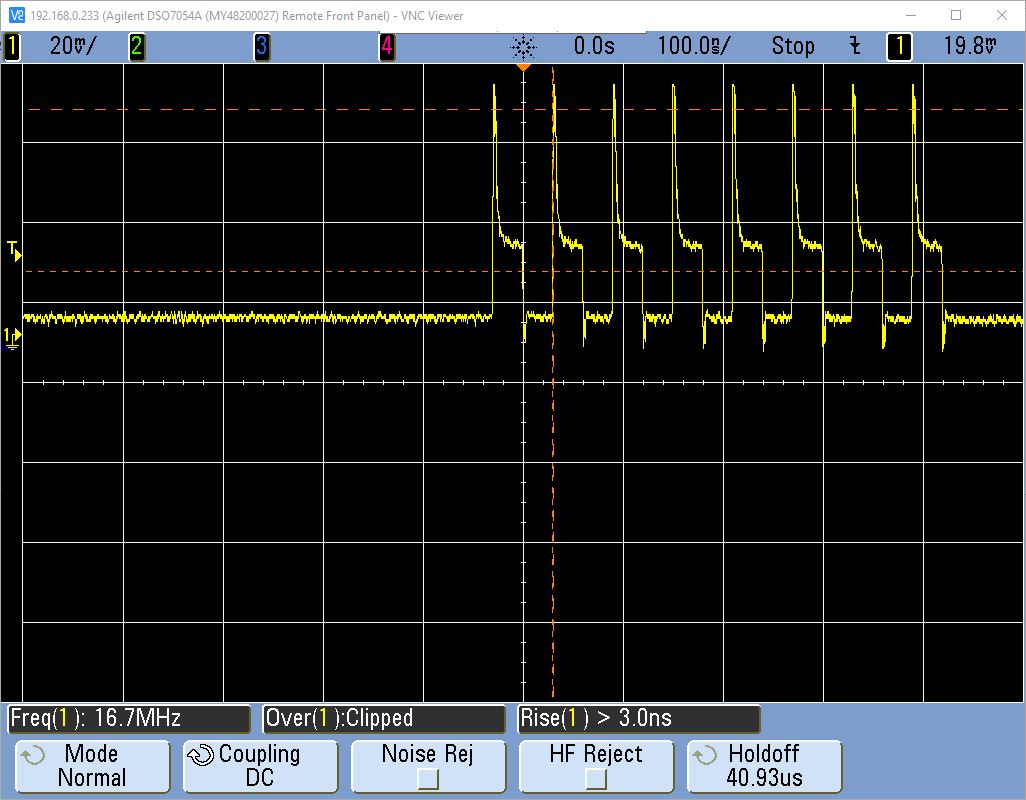
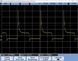
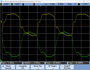
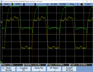
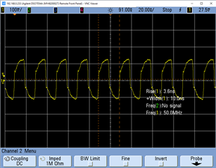
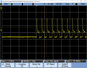
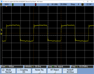
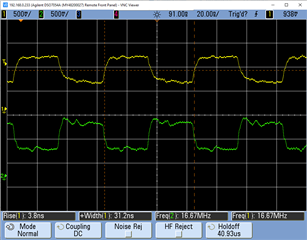
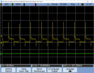
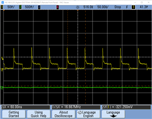
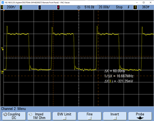
Looking at the output of the LMK04821 SDCLKout using a differential probe (10:1)  I can see the following.

The DCLKout outputs look ok, with a nice waveform. The SDCLKout outputs that are providing the 16.6MHz sysref
look "terrible". Is there something I should set differently?

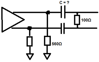
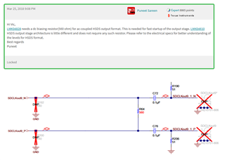
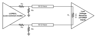
At the outputs of the LMK04821 we have placed 560R shunts, then AC-coupled to the destination and have a 100R termination there (which is actually the sysref input of the AFE58JD18).

Any idea?

Kind Regards,
Ed

  • Hi Ed,

    You mentioned a 10:1 differential probe so maybe I'm not applying the scaling correctly, but it looks like the signal is only 20mVpp (excepting the abnormal excursion). Is this accurate? It almost looks like your outputs are shorted, or else something isn't connected properly and you're looking at feedthrough on a disabled output. Do you have a register programming file for the LMK04821 that I could review?

    Regards,

  • Hi Derek,

    No the V/div is 200mV (I did not adjust the scope scale for the probe), I have added another
    picture (from another board with an LMK04821), now with 20ns/div.

    Regarding the short circuit: it does not measure like a short circuit. By the way, I am using
    4 outputs of the LMK04821 like this, all have the same waveform.

    Sure, the register programming file attached below and I tried to attach  the project file
    for TICS but somehow drag and drop didn't work for that.

    By the way: when measuring single ended on both the SDCLK-p and SDCLK-n it looks like
    the output is the same (instead of the complement of each-other what I would expect for LVDS/HSDS etc).
    Is the SDCLK using a special mode when outputting the SYSREF?

    Kind Regards,
    Ed


    #ifndef __LMK04821__hi_h__
    #define __LMK04821__hi_h__


    #ifndef _lmk04821_reg_t
    #define _lmk04821_reg_t
    typedef struct
    {
        unsigned short reg; /* register number */
        unsigned char  val; /* register data   */
    } lmk04821_reg_t;
    #endif

    #define LMK04821_HI_CONFIG_NUM_REGS  129

    lmk04821_reg_t lmk04821_hi_regs[LMK04821_HI_CONFIG_NUM_REGS] =
    {
        { 0x0000, 0x90 },
        { 0x0000, 0x10 },
        { 0x0002, 0x00 },
        { 0x0003, 0x06 },
        { 0x0004, 0xD0 },
        { 0x0005, 0x5B },
        { 0x0006, 0x00 },
        { 0x000C, 0x51 },
        { 0x000D, 0x04 },
        { 0x0100, 0x14 },
        { 0x0101, 0x55 },
        { 0x0102, 0x55 },
        { 0x0103, 0x01 },
        { 0x0104, 0x20 },
        { 0x0105, 0x00 },
        { 0x0106, 0xF0 },
        { 0x0107, 0x22 },
        { 0x0108, 0x14 },
        { 0x0109, 0x55 },
        { 0x010A, 0x55 },
        { 0x010B, 0x01 },
        { 0x010C, 0x20 },
        { 0x010D, 0x00 },
        { 0x010E, 0xF0 },
        { 0x010F, 0x22 },
        { 0x0110, 0x14 },
        { 0x0111, 0x55 },
        { 0x0112, 0x55 },
        { 0x0113, 0x01 },
        { 0x0114, 0x20 },
        { 0x0115, 0x00 },
        { 0x0116, 0xF0 },
        { 0x0117, 0x22 },
        { 0x0118, 0x14 },
        { 0x0119, 0x55 },
        { 0x011A, 0x55 },
        { 0x011B, 0x01 },
        { 0x011C, 0x20 },
        { 0x011D, 0x00 },
        { 0x011E, 0xF0 },
        { 0x011F, 0x22 },
        { 0x0120, 0x0A },
        { 0x0121, 0x55 },
        { 0x0122, 0x55 },
        { 0x0123, 0x01 },
        { 0x0124, 0x00 },
        { 0x0125, 0x00 },
        { 0x0126, 0xF0 },
        { 0x0127, 0x11 },
        { 0x0128, 0x0A },
        { 0x0129, 0x55 },
        { 0x012A, 0x55 },
        { 0x012B, 0x01 },
        { 0x012C, 0x00 },
        { 0x012D, 0x00 },
        { 0x012E, 0xF0 },
        { 0x012F, 0x11 },
        { 0x0130, 0x0A },
        { 0x0131, 0x55 },
        { 0x0132, 0x55 },
        { 0x0133, 0x01 },
        { 0x0134, 0x00 },
        { 0x0135, 0x00 },
        { 0x0136, 0xFB },
        { 0x0137, 0x11 },
        { 0x0138, 0x38 },
        { 0x0139, 0x02 },
        { 0x013A, 0x00 },
        { 0x013B, 0x3C },
        { 0x013C, 0x00 },
        { 0x013D, 0x08 },
        { 0x013E, 0x03 },
        { 0x013F, 0x0D },
        { 0x0140, 0x00 },
        { 0x0141, 0x00 },
        { 0x0142, 0x00 },
        { 0x0143, 0x10 },
        { 0x0144, 0xFF },
        { 0x0145, 0x7F },
        { 0x0146, 0x10 },
        { 0x0147, 0x1B },
        { 0x0148, 0x33 },
        { 0x0149, 0x42 },
        { 0x014A, 0x02 },
        { 0x014B, 0x16 },
        { 0x014C, 0x00 },
        { 0x014D, 0x00 },
        { 0x014E, 0xC0 },
        { 0x014F, 0x7F },
        { 0x0150, 0x00 },
        { 0x0151, 0x02 },
        { 0x0152, 0x00 },
        { 0x0153, 0x00 },
        { 0x0154, 0x01 },
        { 0x0155, 0x00 },
        { 0x0156, 0x01 },
        { 0x0157, 0x00 },
        { 0x0158, 0x96 },
        { 0x0159, 0x00 },
        { 0x015A, 0x01 },
        { 0x015B, 0x10 },
        { 0x015C, 0x20 },
        { 0x015D, 0x00 },
        { 0x015E, 0x00 },
        { 0x015F, 0x0B },
        { 0x0160, 0x00 },
        { 0x0161, 0x01 },
        { 0x0162, 0xA4 },
        { 0x0163, 0x00 },
        { 0x0164, 0x00 },
        { 0x0165, 0x04 },
        { 0x0171, 0xAA },
        { 0x0172, 0x02 },
        { 0x0173, 0x00 },
        { 0x0174, 0x05 },
        { 0x017C, 0x15 },
        { 0x017D, 0x33 },
        { 0x0166, 0x00 },
        { 0x0167, 0x00 },
        { 0x0168, 0x04 },
        { 0x0169, 0x49 },
        { 0x016A, 0x60 },
        { 0x016B, 0x00 },
        { 0x016C, 0x00 },
        { 0x016D, 0x00 },
        { 0x016E, 0x13 },
        { 0x1FFD, 0x00 },
        { 0x1FFE, 0x00 },
        { 0x1FFF, 0x53 }
    };

  • Hi Ed,

    You have the DCLK and SDCLK set to the same HSDS output format, do you have the same hardware output interconnection like the following? What is the C value? If you set the SDCLKoutx_MUX bit to make SDCLK output become DCLK, will you get a good waveform?

  • Hi Noel,

    The schematic you have drawn is different from the one that I have found earlier on the TI site, see below.

    The 560R is on SDCLKout_P and SDCLKout_N. The capacitors are 100nF.

    >> If you set the SDCLKoutx_MUX bit to make SDCLK output become DCLK, will you get a good waveform?

    Yes then I can see what I would expect and that is exactly the same as the signal from DCLK.

    I have also measured directly on the chip (so "before" the capacitors), the P & N output are in phase then instead of inverted.

    Kind Regards,

    Ed

  • Hi Ed,

    Since you were saying 560Ω shunts, I thought you have a shunt at each pin. The schematic in the EVM user's guide is correct, the 560Ω resistor should be placed across the pins. 

    I don't have idea why switching to SDCLK will generate issue, let me check with other team member and get back.

  • Hi Noel,

    We have a 560R shunt on every used output of the LMK04821, hence shunts.

    All these outputs are configured the LVDS or HSDS6.

    Thanks in advance.

    Kind Regards,

    Ed

  • Hi Noel,

    I have acquired some scope pictures

  • Hi Noel,

    I have acquired some scope pictures

    Single Ended DCLK

    Single Ended SDCLK

    Differential DCLK

    Differential SDCLK

    All measured directly on chip (of course with the earlier explained circuit on the "other" side).
    Just to make certain the capacitors will not cause any change on the signal.

    I hope this clarifies what I am observing here.

  • Hi Ed,

    so you are seeing unbalanced waveform between _P and _N pins, could you verify, if you put DCLK = 16.67 MHz, you will also see the uneven waveform? If this is the case, can you increase the AC-coupling capacitor to 1µF?

  • Hi Noel,

    I have been reading some other issues with the LMK04821 on this forum and one situation
    striked me was the one that exactly described what I was seeing on the scope.

    That is: P & N exactly in phase, while we would expect the N to be the inverted one of P.

    The only thing "they" did to "solve" this was set the SYSREF in continuous mode.

    So I thought: let's place the SYSREF in continous mode, 0x0139 0x02 => 0x03

    Then I have obtained the new scope-pictures as below:

    So what is happening when using pulsed sysref?

    By the way: I have measured waveforms from previous post directly on chip.

    Kind Regards,

    Ed

  • Hi Ed,

    Let me check with my team and get back.

  • Hello Ed,

    I was reviewing the images.  My understanding is the signal looks bad and low amplitude with the diff probe because the outputs are in same-phase, so you're measuring the delta voltage of this same-phase clock.

    Can you confirm you see this for both LVDS and HSDS x mA signals?  Any difference if you use different levels of HSDS?

    I'm wondering if for the continuous sysref, if you were to trigger your scope on the rising CS*, would you see the same phase to correct phase transition.

    One more test I would request, could you replace the 560 ohm resistor with a 100 ohm resistor?

    73,
    Timothy

  • Hi Timothy,

    >>I was reviewing the images.  My understanding is the signal looks bad and low amplitude with the diff probe because the outputs are in same-phase, so you're measuring the delta voltage of this same-phase clock.

    Your observations are correct.

    >> Can you confirm you see this for both LVDS and HSDS x mA signals?  Any difference if you use different levels of HSDS?

    I have tried it with HSDS6 and LVDS, same result....
    By the way have a look at

    https://e2e.ti.com/support/clock-and-timing/f/clock-timing-forum/914389/lmk04821-convert-sysref-output-to-single-end-to-drive-lmg1020

    He has 2 signals in phase as the output from SYSREF

    And here

    https://e2e.ti.com/support/clock-and-timing/f/clock-timing-forum/882012/lmk04832-lmk04832-sysref-clock-problem

    Where there is a complaint about difference in amplitude for the SYSREF pos and neg side.

    >> I'm wondering if for the continuous sysref, if you were to trigger your scope on the rising CS*, would you see the same phase to correct phase transition.

    Yes..... the probe used for the single ended measurements are not active and a short probe GND-cable ruins the signal.
    The differential probe is up to 800MHz and has very short pins (~ 0.5 cm) so the signal is ok!
    (except for the differential DCLK where the probe impedance wasn't set correctly at the scope)

    >> One more test I would request, could you replace the 560 ohm resistor with a 100 ohm resistor?
    This is a bit harder to do since these are 0402 resistors glued onto the board, I had verified with TI that the shunt of 560R would be ok, isn't that ok?  TI has an EVM with the LMK04821, can you check with that one if the signal coming from the SDCLK outputs is equal (signal quality/standard wise) to the DCLK when outputting a pulsed SYSREF?

    By the way, I have also tried to output the SYSREF pulsed (8 pulses) but then with a very short interval ( ~ 15 microseconds from eachother) so that if there would be any charging/decharging of the capacitors that would be a problem it would show as some kind of a ramp
    on the signal... but no, no ramp.

    So:

    => with DCLK muxed to SDCLK = signal OK

    => with SDCLK distributing continuous SYSREF = signal OK

    => with SDCLK distributing pulsed SYSREF = signal crappy

    Looking forward to hearing from you.

    Kind Regards,
    Ed

  • Timothy,

    I have acquired a picture with HSDS10 and for ref HSDS6 with diff probe

    HSDS10

    HSDS6

    As you can see there's more overshoot/undershoot at HSDS10.

    No other special observations.

    Kind Regards,

    Ed

  • See scope pictures below.

  • Hi Timothy,

    I have placed a resistor in parallel of the 560R shunt resistor so that the resulting resistance is ~ 100R.

    Then the signal looks good (see attached picture where I have configured V/div correctly, the amplitude is ~ 600mV which is exactly what it should be for HSDS6).

    Question remains: why does this shunt resistor needs to be so low.... while TI advise is to use 560R?

    Another question is: why are we the "first" ones to encounter this?

    Kind Regards,

    Ed

  • Hello Ed,

    Question remains: why does this shunt resistor needs to be so low.... while TI advise is to use 560R?

    My understanding is that when you AC couple, without the 560 ohm resistor the relationship between the voltage on two outputs can diverge and cause the driver some start-up delay.  By placing the 560 ohm this allows a DC path for the driver to help prevent this start-up delay.  Note, even when you placed the resistor to cause the start-up to occur faster, there is still a delay before the receiver's input DC balances.
       * The recommended method to eliminate delay and to use SYSREF pulser would be to DC couple.  Otherwise the input signal may still not be valid due to the lack of DC balance.  For example in the image below, the top is the probe DC coupled to the transmitter.  But the receiver sees the other waveform as it DC balances.  Would the Vod1, Vod2, Vod3 measurements meet the requirements for the receiver?

    The continuous SYSREF mode is recommended for AC coupled SYSREF.  This allows the AC coupled differential waveform to DC balance before the JESD204B receiver uses the SYSREF to deterministically mark the device clock.  If you use smaller capacitors then the balancing will occur faster.

    I realize this answer doesn't directly address the same-phase issue except for lumping it into the delayed start-up time for DC balancing.  At this time I can only suggest the 100 ohm termination would ensure the start-up without the out of phase clock.  This however this would result in a lower amplitude clock because of higher loading, since you are using HSDS 6 mA, you may be able to compensate by increasing to a higher HSDS level.  The best case would be to turn off the 100 ohm load in receiver, and place the 100 ohms close to the load with the DC blocking capacitors directly between load and IC.

    If DC coupling LVDS doesn't work, then consider the LCPECL output format and termination I suggest in the next portion of this response.

    Another question is: why are we the "first" ones to encounter this?

    My understanding is that the 560 ohm resistor solves the start-up issue.  I don't think anyone has run into this issue with SYSREF as it is not advised to AC couple SYSREF in pulser mode.  The LMK05828 supports an output format LCPECL for low common-mode PECL.  This output is designed to have relatively high swing (Vod = 0.95 V) with low relatively low common mode (1.1 V)

    If you create a voltage divider from the emitter resistor then you can reduce the Vcm to lower levels required by some low voltage parts.  Note that Rb one one leg is in parallel with RL + Rb of other leg.

    This would be the method recommended for using SYSREF in pulser mode for inputs which require common modes less than an LVDS output can provide.

    Hope this helps Ed.

    73,
    Timothy