Other Parts Discussed in Thread: OPA188
Hi, we have design a board that use ADS1258 ADC to convert 8 differential channel.
We have a problem only when we use channel 0 and channel 7 together.
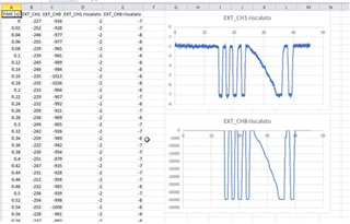
We have wired on channel 0 a load cell (5V supply), on channel 7 a linear potentiometer (5V supply).
When potentiomer change from 0 to full scale, on channel 0 there is a variation of about 5-7 point (on about a scale of 45000 point).
Swapping the sensors position, potentiometer on channel 0 and load cell on channel 7 the problem is the same.
But leaving load cell on channel 0 and placing potentiomer on any channel from 1 to 6 the problem disappears.
Also leaving potentiometer on channel 7 and placing load cell on channel 1 to 6 the the problem disappears.
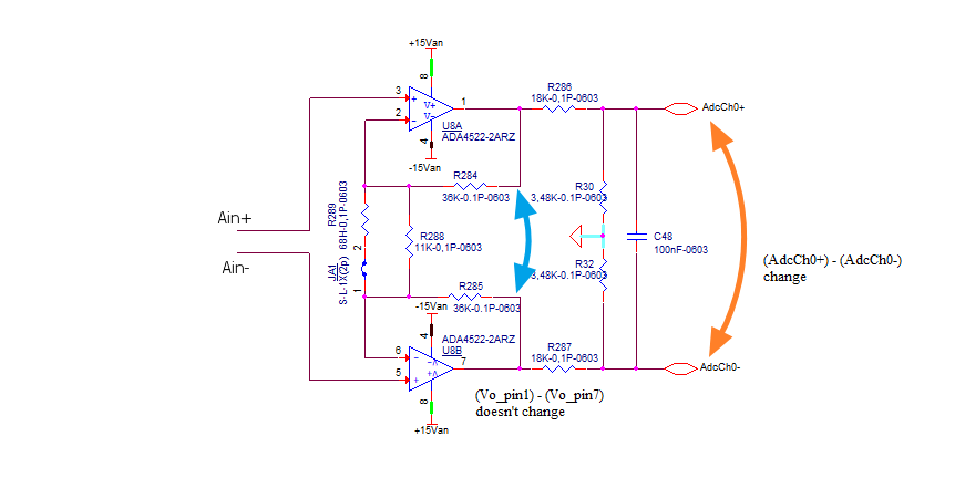
All analog stage before adc are the same.
As first, i have think to some trace coupling problems.
But on the pcb, channel 0 and 7 are placed at the maxium distance,
Also note that this design is a remake of a previous existing design that use AD7779 (the design has been redone because AD7779 in not available at this time).
With AD7779 no problems.
The pcb routing is the same (from input connector to IA, and from IA output until near adc input the differential trace routing are the same on the 2 pcb revision), obviously excluding the area near the ADC.
Someone have some ideas ?? channel 0 and channel 7 also have opposite position on the chip!!
thanks in advance.