Hello everyone! We use custom board with Kintex-7 FPGA and DAC3171 with 14-bit data bus (Fs = 250 MHz, two's complement ). During DAC3171 setup we noticed that lower 7 data pins (D[6:0]) make no impact onto the output analog signal. Only when the digital signal level exceeds 127 (occupy more then 7 LSB bits), we can see analog output changing - this is the problem. It seems like only 7 MSB pins (D[13:7]) work.
We have done a couple of tests:
TEST 1. Using config20 register we tried to get a constant analog output changing according to sifdac value. Ascending sifdac value from 0 to 127 we have seen the same very low DC signal all the time. Right after D[7] become no longer a sign bit, analog signal had started to ascent too. We used oscilloscope to measure output voltage
TEST 2. We used iotest with 8 different patterns and 8 equal patterns coming from FPGA with SYNC signal. All the pins passed the test successfully according to config4 = 0x0000 (this register was cleared during the test). Making an error in any pattern make desired pin to fail the test as we expect.
TEST 3. Trying to transmit different constants from FPGA we had no success with D[6:0] too. Only 7 MSB bits (D[13:7]) worked well.
We use power-up sequence from datasheet to configure the DAC (7.5.1 p.38 in the last revision).
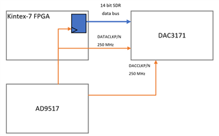
Pins SLEEP, TXENABLE and RESETB a well-controlled by FPGA (tested with oscilloscope). Clocks DATACLKP/N and DACCLKP/N are equipped with 250 MHz clocks from AD9517 before the DAC configuration starts. Timings of data bus are observed (FPGA delays DATACLKP/N signal for 1 ns to move the rising edge to the center of data). ALIGNP = DIGVDD18, ALIGNN = GND according to datasheet as we don't use them. SYNCP = 0, SYNCN = 0 by FPGA as we use sif_sync feature for DAC internal FIFO synchronization.
Few people encountered alike problems:
https://e2e.ti.com/support/data-converters-group/data-converters/f/data-converters-forum/416334/dac3171-configuration-problem (right the same problem)
https://e2e.ti.com/support/data-converters-group/data-converters/f/data-converters-forum/536109/dac3171-with-incorrectly-programmed-fuses
https://e2e.ti.com/support/data-converters-group/data-converters/f/data-converters-forum/416232/dac3171-7-bit-interface-mode
Do we have any troubles with internal DAC fuses? Our DAC3171 marks are:
TI 83J
PJ5J G4
Such registers values generated by TI DAC3174 EVM GUI are used:
{addr=0x00, data=0x46e4},
{addr=0x01, data=0x600f},
{addr=0x02, data=0x3fff},
{addr=0x03, data=0x0000},
{addr=0x04, data=0x0000},
{addr=0x05, data=0x0000},
{addr=0x06, data=0x0000},
{addr=0x07, data=0xffff},
{addr=0x08, data=0x6000},
{addr=0x09, data=0xe000},
{addr=0x0a, data=0xf080},
{addr=0x0b, data=0x1111},
{addr=0x0c, data=0xffff},
{addr=0x0d, data=0xffff},
{addr=0x0e, data=0xffff},
{addr=0x0f, data=0xffff},
{addr=0x10, data=0xffff},
{addr=0x11, data=0xffff},
{addr=0x12, data=0xffff},
{addr=0x13, data=0xffff},
{addr=0x14, data=0x8000},
{addr=0x15, data=0x0000}Here it is simplified schematic of our board (SLEEP, TXENABLE and RESETB are connected to the FPGA too):Best Regards
Nick H.

-
Ask a related question
What is a related question?A related question is a question created from another question. When the related question is created, it will be automatically linked to the original question.