A related question is a question created from another question. When the related question is created, it will be automatically linked to the original question.
If you have a related question, please click the "Ask a related question" button in the top right corner. The newly created question will be automatically linked to this question.
ADS1298R: Cannot generate internal square wave test signal
Configuration register 2 provides pulses not square waves, isn't it?
If I choose external test signals, does it mean I should provide test signals as input? Is there any difference between providing square waves as normal input and as external test input?
May I ask do you happen to have/use an ADS1298R evaluation kit/board(EVM)?
Could you take a look of EVM user guide
"4.2 Internal Test Signals Input Configuration Register 2 controls the signal amplitude and frequency of an internally-generated square wave test signal. The primary purpose of this test signal is to verify the functionality of the front-end MUX, the PGA, and the ADC. The test signals may be viewed on the ECG Display tab, as Figure 31 shows. Detailed instructions for using the ECG Display tab are provided in Section 3.5.5."
and to see whether that is the square wave you are referring to?
It makes sense for "send SDATAC, there are pulses on the DRDY pin.... ".
As SDATAC means the host/master is asking the ADS to convert&read the the signal/data continuously, and DRDY pin is used to indicate whenever the converted data is ready to be read by host/master.
It is said that "This SDATAC opcode command cancels read data continuous (RDATAC) mode. " in datasheet on page 63. I thought this command is asking the ADC to stop convertion. And DRDY will stay high.
What will happen if AVDD-AVSS = 2V? In 7.1 minimum AVDD-AVSS is -0.3 but in 7.3 the recommended minimum is 2.7V. If AVDD-AVSS = 1.57V, it is unacceptable? And why?
"It is said that "This SDATAC opcode command cancels read data continuous (RDATAC) mode. " in datasheet on page 63. I thought this command is asking the ADC to stop convertion. And DRDY will stay high."
Yes. That's correct.
Do you send the SDATAC opcode command just once?
"CLKSEL is linked to DVDD and START is pulled high upon the ADC powered up."
CLKSEL=1 means internal clock is used.
What are the RESP_CTRL[1:0] settings? Please note - (1) Do not set RESP_CTRL[1:0] = 11 if CLKSEL = 1 (internal master clock).
if START is pulled high by circuit/hardware, please make sure to check the data sheet "9.4.1.1 Start Mode Pull the START pin high for at least 2 tCLK periods, .... to begin conversions." and 9.4.1.1.1 Settling Time and 9.4.1.2 Data Ready Pin (DRDY).
"What will happen if AVDD-AVSS = 2V? In 7.1 minimum AVDD-AVSS is -0.3 but in 7.3 the recommended minimum is 2.7V. If AVDD-AVSS = 1.57V, it is unacceptable? And why? "
AVDD-AVSS=1.57V may not work properly as it's outside the Recommended Operating Conditions, thus, TI cannot guarantee and performance if the usage does not follow/meet the data sheet requirements.
7.1 indicates the range that prevent/avoid damaging the device; 7.2 indicates the range for the device to work/operate properly.
For now, Can you read the ID register's device ID correctly?
How is the RESET pin connected?
In the meantime, please take a look of this thread to see whether you need to debug/troubleshoot the SPI communication.
Yes, I send SDATAC only once. Should DRDY stay high or is it ok even if there are pulses?
I'm not sure about RESP_CTRL[1:0]. I didn't set RESP register. I think it stays as default, 00 maybe.
RESET is pulled high all the time. After reading 11.1, I add a delay before RESET pulled high. Then RESET is pulled low for some time and then pulled high again. I think the delay meets the minimum requirements.
Then I send SDATAC and RREG. I changed the number of registers I want to read but the data I got is always the same.
I checked the AVDD-AVSS and DVDD again. DVDD = 2.5V, AVDD-AVSS = 3V.
Could you please check(Zoom-In) whether DIN stable(Not change) for at least tDIST before the falling edge of the SCLK?
Make sure SCLK falling edge and DIN's edges never align/overlap.
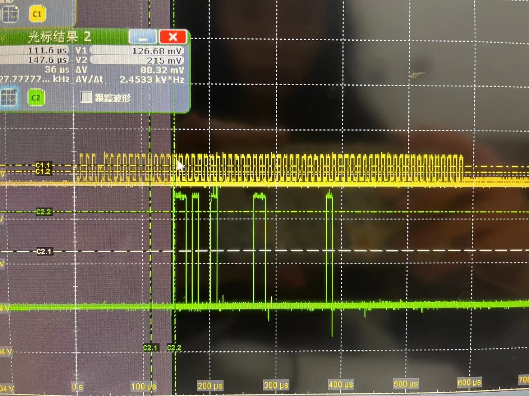
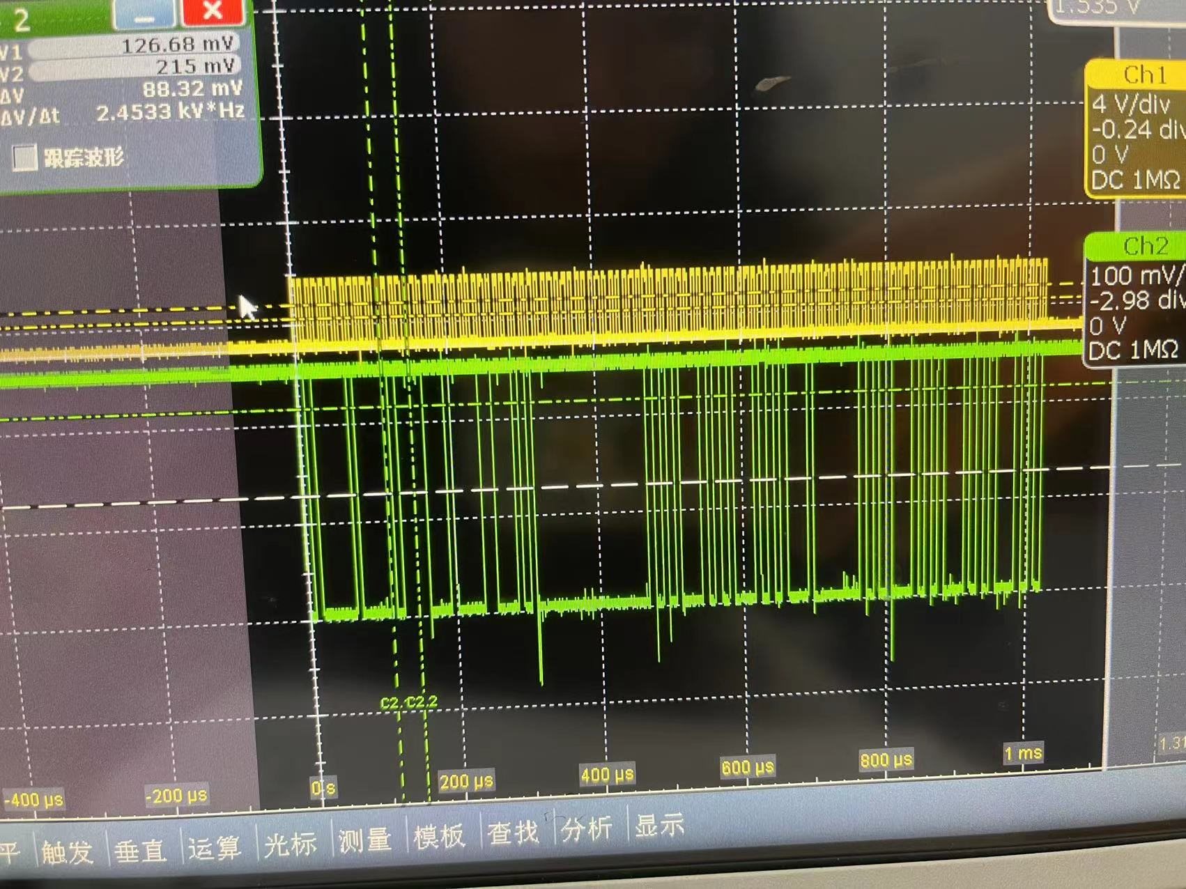
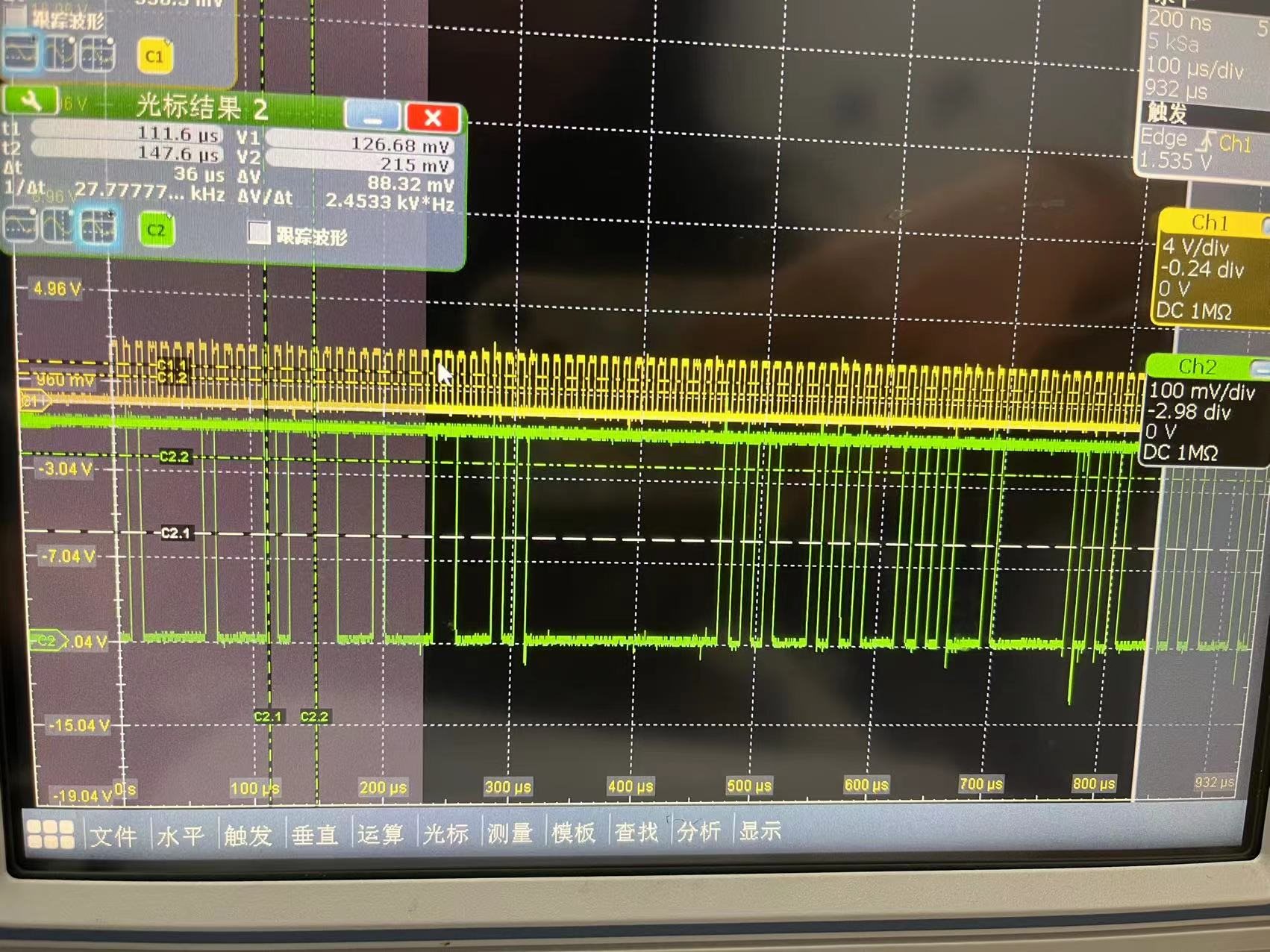
"Before writing to registers, I got 0x00 0x00 0xd2 0x06 0x00 0x40 if I want to read ID register"
So, from the scope, does the DOUT signal clocked by the SCLK match what you expect for the ID register?
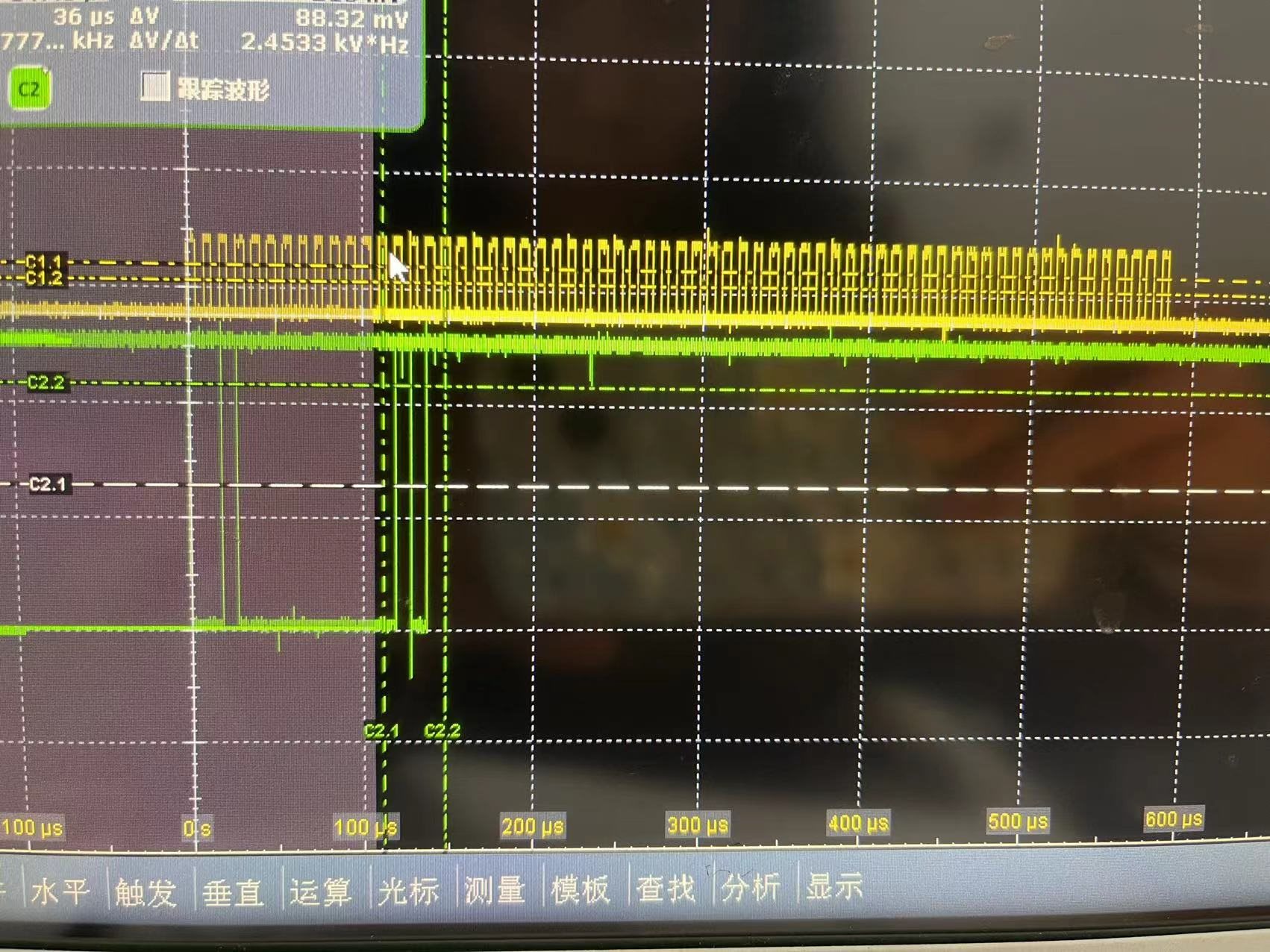
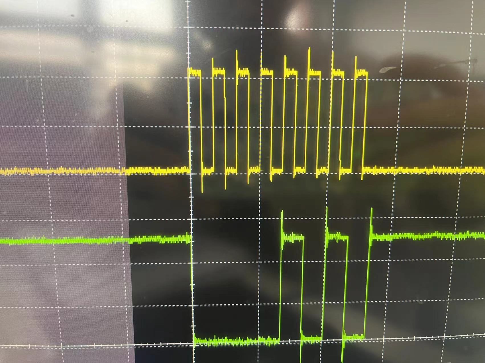
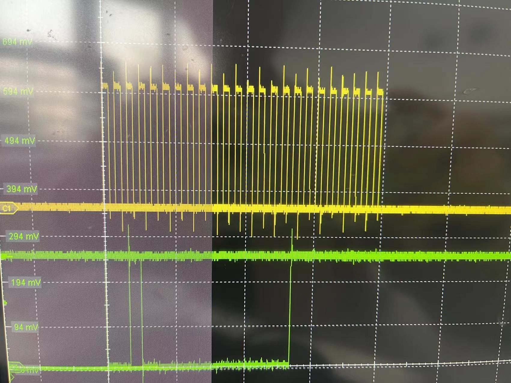
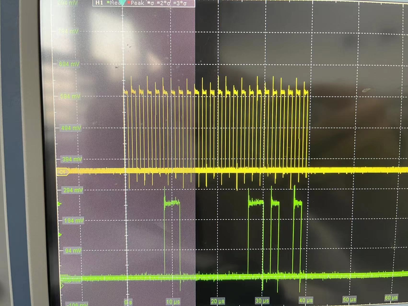
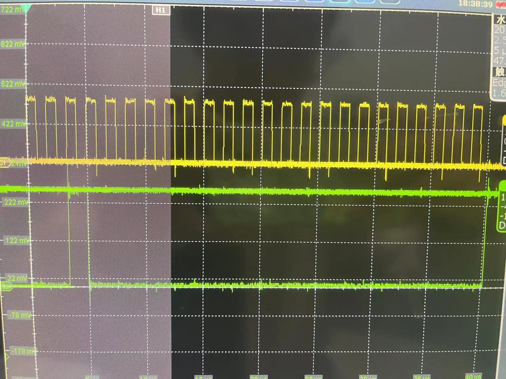
"But the DOUT of ADC is changing all the time. Green line is DOUT and yellow line is SCLK."
During this time, do you send any command to DIN? and What was the START pin setup/connected?
What were your Channel settings/configurations? Do you configure it to read the test signals?
It makes sense for the DOUT to change slightly as even for a steady signal, there might be some fluctuation/variation in the LSBs. But, could you please check(zoom-in) to see whether the SCLK's falling edges do not align/overlap with the DOUT's edges.
Could you do the following checks?
1. Read 9.6.1.1 ID: ID Control Register (address = 00h) and make sure from both the scope and your host can read the correct value according to the datasheet?
2. If above works correctly, try write and read 9.6.1.6 CHnSET: Individual Channel Settings (n = 1 to 8) (address = 05h to 0Ch) (reset = 00h), validate only 1 channel first, e.g. channel 1, during which please watch the scope to make sure the SCLK and SPI lines can clock at the correct logic high and/or low levels.
If possible, please provide picture(preferred Zoom-In) for above two.
First, I pulled RESET high. After about 25ms, I pulled RESET low for 12.5ms. Then I pulled RESET high again. After 25ms, I pulled CS low and send SDATAC. Then I start to send RREG periodically to read ID register. The clock rate of SCLK is 655kHz. START pin is 0 and never changed.
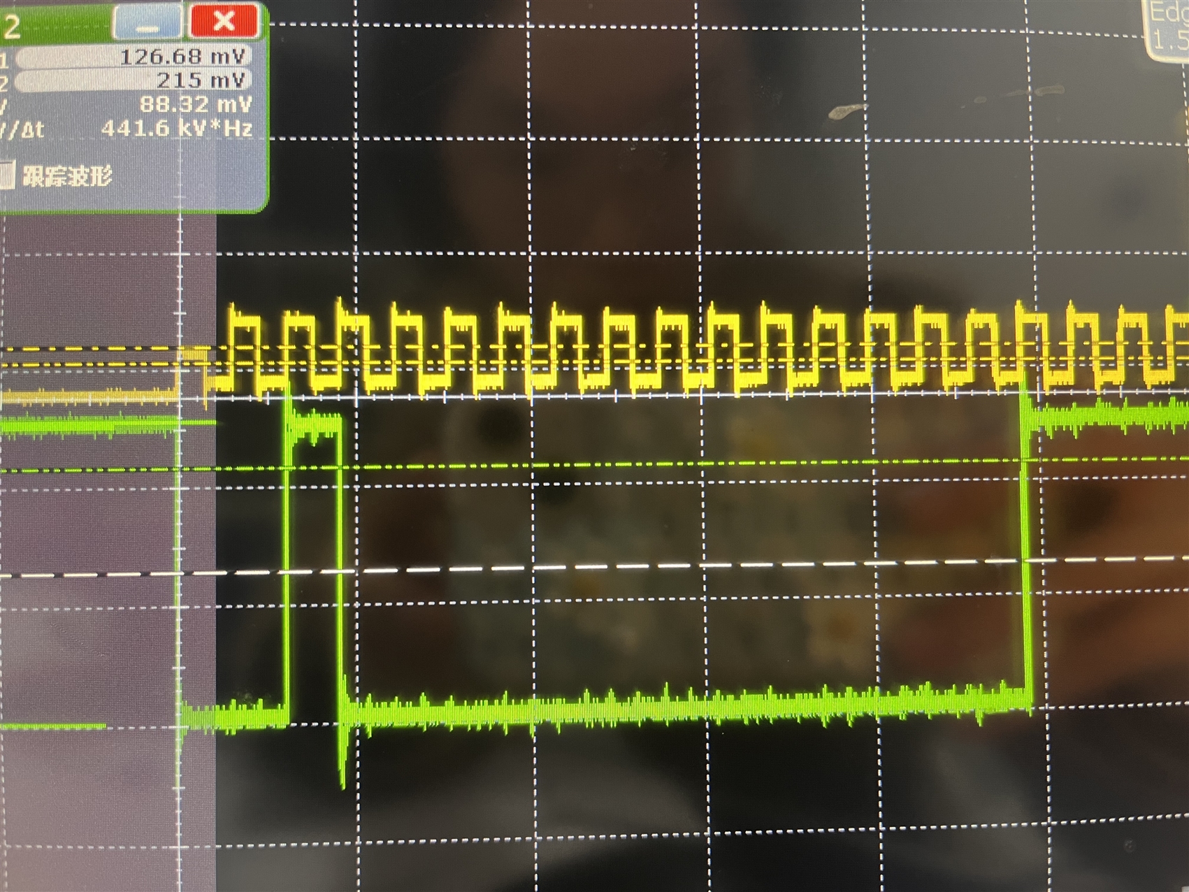
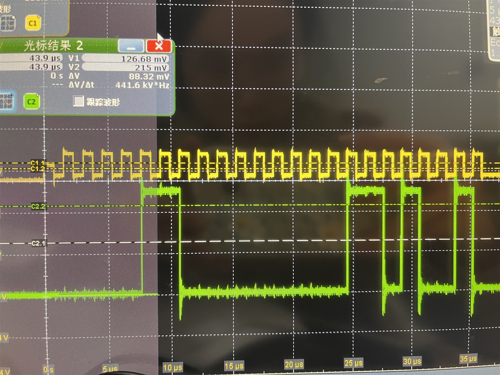
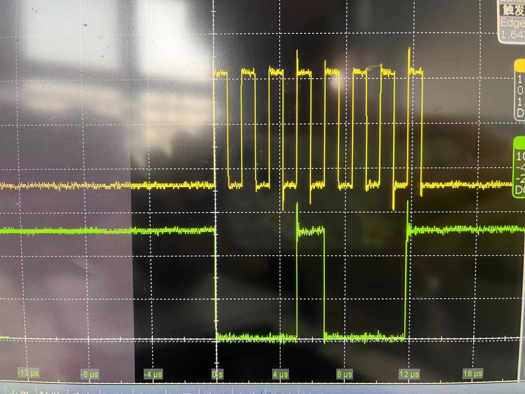
This is DIN and SCLK. I send 0x20 0x00 0xFF to read ID register.
This is DOUT and SCLK. Then I got 0x06 0x00 0xd2.
I think DIN and DOUT are steady. Both signals don't change on the falling edge. And RREG command is issued every 12.5 ms. There should't be any overlap.
And what does it mean "/ If VCAP1 < 1.1V at t , continue waiting until VCAP1 1.1V" in the datasheet on page 85?
VCAP1 - AGND = -300mV, VCAP1-AVSS= 1.2V. Does it meet the requirement?
By the way, could you double check on your board that there is not other oscillator clock that is conflicting/competing with the ADS internal clk?
For, "After 25ms, I pulled CS low and send SDATAC. Then I start to send RREG periodically to read ID register. The clock rate of SCLK is 655kHz. START pin is 0 and never changed."
Could you show me how the scope signals look like for
SDATAC Stop Read Data Continuously mode 0001 0001 (11h)
and
Could you also try to send
STOP Stop conversion 0000 1010 (0Ah)?
Are they being clocked to DIN correctly?
For "Then I start to send RREG periodically to read ID register. "
So, do you see the correct ID register value on the scope? Refer to Table 17. ID Control Register Field Descriptions
it might be 110 10 010 = D2h for ADS1298R
Then, if your reset is proper, try to see if you can read 9.6.1.2 CONFIG1: Configuration Register 1 (address = 01h) (reset = 06h) on the scope.
If above two work, then try to see if you could read both 00h and 01h registers(i.e. same as the two registers above) together by following
Figure 72. RREG Command Example: Read Two Registers Starting from Register 00h (ID Register) (OPCODE 1 = 0010 0000, OPCODE 2 = 0000 0001)
and observe whether the values look correct on the scope.
For, "/ If VCAP1 < 1.1V at t , continue waiting until VCAP1 1.1V" in the datasheet on page 85?
The VCAP needs to charge up to 1.1V to properly allow /reset the device; please take a look of the Figure 105. Power-Up Timing Diagram
So, please make sure all the VCAPs on your board meet the required value on the datasheet
and make sure you wait at least 2^18 of the tCLK before pulling the /RESET to low for at least 2 tCLK,
i.e. if you are using internal-oscillator clock, it's 2.048MHz, so the tCLK is around 0.4883 us, so you may need to wait for at least 128005 us before pulling the /RESET to low.
If all above works correct, then try to read 9.6.1.3 CONFIG2: Configuration Register 2 (address = 02h) (reset = 40h) on the scope to see whether the reset value looks correct on the scope.
Then, write 1 to 02h[4], i.e. bit 4 and then read the register value back observe on the scope.
Could you make sure above all work, then we can move on to
9.6.1.6 CHnSET: Individual Channel Settings (n = 1 to 8) (address = 05h to 0Ch) (reset = 00h), but just one channel(e.g. Channe1 CH1SET) at a time.
1. "By the way, could you double check on your board that there is not other oscillator clock that is conflicting/competing with the ADS internal clk?"
SDATAC Stop Read Data Continuously mode 0001 0001 (11h) on DIN looks correct.
STOP Stop conversion 0000 1010 (0Ah) on DIN looks correct.
2. May I ask why do you have/send "0xFF" in "Then I send RREG to read ID register only. This is DIN 0x20 0x00 0xFF"?
Understood that CLKSEL is linked to DVDD and START is pulled high upon the ADC powered up.
3. So, is the START pin controlled by the host/master device's digital signal?
4. Does the START pin have a pull up resistor to DVDD and also have signal line connect/go to one of the master/host's digital line?
5. Does the CS pin have a pull up resistor to DVDD and also have signal line connect/go to one of the master/host's digital line?
6. Before and After RESET, Could you pull the START pin to low and keep the START pin low?
As, when the START pin is high or the START command is sent, the A/D conversion begins and the /DRDY from ADS will keep pulsing/triggering.
For now, I may suggest keeps START pin low and only use command to START and/or STOP.
7. If you try to read only 9.6.1.1 ID: ID Control Register (address = 00h); Refer to Table 17. ID Control Register Field Descriptions, Do you read/get 110 10 010 = D2h for ADS1298R?
1. "By the way, could you double check on your board that there is not other oscillator clock that is conflicting/competing with the ADS internal clk?"
2. The SCLK is still clocking into the ADS, which may cause some unexpected performance.
3. "START pin is initialized with 0. And it is never pulled high during the test." OK.
And, please take a look of the attached PDF, see if you can verify/validate that your WREG commands works, e.g. to configure for the internal test signal.
And, see if you can try the START command and RDATAC command.