This thread has been locked.
If you have a related question, please click the "Ask a related question" button in the top right corner. The newly created question will be automatically linked to this question.
Srinivas (Hope that this gets to you),
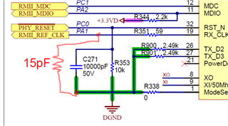
We are moving forward with changing our design to use the DP83826 PHY based on TI's recommendation and our series of testing with the DP83826EVM from our previous thread.
The updated design is attached which replaces the LAN8742A with the DP83826. As discussed previously we are looking forward to your input on the design before we commit to our next build.
Hope that you are doing well - look forward to hearing from you soon.
Take care - Duncan
Hello Duncan,
Thank you for the message and good to know the progress.
I will review and provide my inputs by early next week.
Take care,
Regards,
Sreenivasa
4857.DP83826 PHY Review Copy - Schematic_10101.B_2021-07-20.pdf
Hello Duncan,
I have embedded the comments in the attached schematic PDF.
Summary includes terminating unused TX_ signals, MDI transformer CT termination caps, CEXT cap value change and some additional suggestion for performance improvements.
Regards,
Sreenivasa
Sreenivasa,
Thanks for your inputs. I have some questions.
"Considering TX_D2, TX_D3, TX_CLK use a 2.49K": Are you referring to pins 26, 27 and 22? I assume that these should be pulled to GND with the 2.49k? Even those these signals are not used in the RMII mode is this just good practice to not leave them floating?
"Please check crystal load cap - TI recommends 15 - 40 pF": The 22 pF values and crystal p/n were copied from the DP83826 eval board which I assume is a good starting point.
"Please check the capacitor value, a 2-nF cap is recommended. Reference section 7 Pin Configuration and Functions (BASIC Mode)": The 0.1µF value was copied from the DP83826 eval board. 2 nF is quite a big difference but I’ll make that change.
I noticed that the 50Ω pull-ups to VDDA3.3 on TD_P/M & RD_P/M were left on the board when I was testing with the DP83826 eval board but it does not look like those are required and have been removed from the design. Could those pull-ups have been an issue with the eval board test and prevented the 100M mode working while 10M was working OK?
Appreciate your help - Duncan
Hello Duncan,
Thank you for the query.
"Considering TX_D2, TX_D3, TX_CLK use a 2.49K": Are you referring to pins 26, 27 and 22? I assume that these should be pulled to GND with the 2.49k? Even those these signals are not used in the RMII mode is this just good practice to not leave them floating?
You are correct.
"Please check crystal load cap - TI recommends 15 - 40 pF": The 22 pF values and crystal p/n were copied from the DP83826 eval board which I assume is a good starting point.
Should be OK but this was a note for you. Parasitic capacitance adds.
"Please check the capacitor value, a 2-nF cap is recommended. Reference section 7 Pin Configuration and Functions (BASIC Mode)": The 0.1µF value was copied from the DP83826 eval board. 2 nF is quite a big difference but I’ll make that change.
Ok
I noticed that the 50Ω pull-ups to VDDA3.3 on TD_P/M & RD_P/M were left on the board when I was testing with the DP83826 eval board but it does not look like those are required and have been removed from the design. Could those pull-ups have been an issue with the eval board test and prevented the 100M mode working while 10M was working OK?
Would it be possible to do a quick check?
Regards,
Sreenivasa
Sreenivasa,
Final DP83826 schematic is attached and would appreciate one last check from you. Your input has been very helpful.
We were not able to test without the 50Ω pull-ups as the prototype board we were using is no longer available.
Getting very close to the end of this design update. Our biggest challenge at the moment is finding parts so we can build and test units and there are no easy answers to getting around that in the short term.
Take care - Duncan
Hello Duncan,
Thank you for the message and sorry to hear on some of the challenges you have been facing.
I will provide my inputs by end of the week.
On a quick review, i saw that the pin21 powerdown/interrupt not connected. I would suggest to pull up the pin with a 2.2K resistor.
Regards,
Sreenivasa
Hello Duncan,
In addition to the above here are a couple of inputs
Please check voltage rating for c275 and C902, C903, C904 .
We recommend a single or dual channel TVS on the LED pins. This depends on the EMI/EMC requirements you might have.
I would consider having a series resistor for the MDIO signals although not a must.
The Cext cap of 2.2nF should be fine.
I also assume the TX terminations are place near to the MCU/SOC.
Good luck for your design.
Regards,
Sreenivasa
Hello Duncan,
Can you please provide a place holder for a 15pF cap for pin 19 after R351. You can make that cap as DNP to start with.
Regards,
Sreenivasa
Sreenivasa,
Yes. I can add a 15 pF cap as you suggest. I assume that the cap should connect between the uC side of R351 and DGND as shown below. What situation would require this cap to be installed and not just DNP?
Thanks - Duncan
Hello Duncan,
Thank you for the inputs and this is correct.
If there are performance issues in terms of packet errors, you could consider mounting this cap and testing.
Regards,
Sreenivasa