This thread has been locked.

If you have a related question, please click the "Ask a related question" button in the top right corner. The newly created question will be automatically linked to this question.

DP83640: AFBR-5803AZ- 100FX fiber interface with Resistor N/W COnformation

Part Number: DP83640
Other Parts Discussed in Thread: DP83869HM, DP83869, TIDA-00928, TIDA-00496, , TIDA-00306

Hi All,

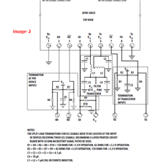
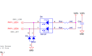
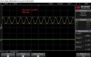
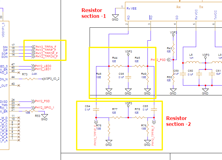
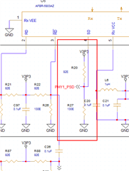
In my project, I need to interface the DP83869HM to the AFBR-5803AZ 100FX fiber module.

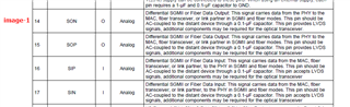
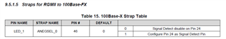
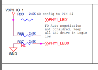
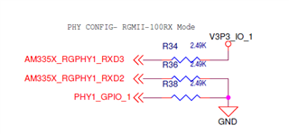
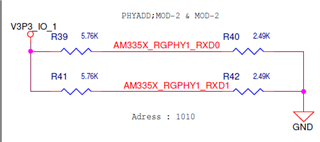
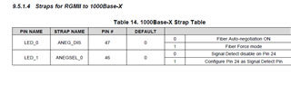
Please refer to the below schematic section and confirm whether required two sets of Resistor divider network in between the Phy to FIber signal.

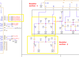
Also, I have attached a schematic of the PHY and 100FX fiber module section in PDF format.6864.schematic.pdf

Regards

Anees PK.

  • Hi Anees,

    The fiber termination resistors may be used to convert two different types of signaling, for example LVDS to LVCMOS. These are application dependent and fiber transceiver dependent. If you know the signaling used from the fiber transceiver you may be able to select you fiber termination resistors appropriately. 

    Thank you,

    Nikhil

    All information in this correspondence and in any related correspondence is provided “as is” and “with all faults”, and it is subject to TI’s Important Notice (http://www.ti.com/corp/docs/legal/important-notice.shtml).

  • Hi Nikhil,

    Thanks for the details.

    Please confirm the following also.

    • As per the datasheet of DP83869 , this SOP and SIP pinas are LVDS and add 01f decoupling cap. Not mentioned adding any additional matching resistors in the PHY chip side.  Please refer to the below images-1
    • On the fiber transceiver side, mentioned adding Termination signals. Refer to the below image-2. The FIber side not mentioned the type of signs but given the signal level, (It is in LVDS range ). Fiber module Vcc is 3.3V. Fiber module data input electrical are also given below.

    So we can remove the termination resistor on the Phy side and keep the termination mentioned on the FIber side. Please confirm. 

    Regards

    Anees PK

  • Hi Anees, 

    The AC coupling caps will take care of any DC offset. The PHY has internal terminations and the external terminations on the PHY side may no be necessary. Should the SFP require external terminations, then you may keep the terminations on the SFP side.

    Please let me know if you have any further questions, else I will close this thread.

    Thank you,

    Nikhil

    All information in this correspondence and in any related correspondence is provided “as is” and “with all faults”, and it is subject to TI’s Important Notice (http://www.ti.com/corp/docs/legal/important-notice.shtml).

  • Hi Nikhil,

    Thnaks for the detils.

    So I will remove the termination on the PHY side and Keep the series capacitor(0.1uF as per the datasheet ). But keep  the termination on the SFP side(AFBR-5803AZ- 100FX module ).

    Regards

    Anees PK 

  • Hi Anees,

    Yes this should be ok.

    Thank you,

    Nikhil

    All information in this correspondence and in any related correspondence is provided “as is” and “with all faults”, and it is subject to TI’s Important Notice (http://www.ti.com/corp/docs/legal/important-notice.shtml).

  • Hi Nikhil,

    The proto board is not responding with AM335x controller.

    Please help on the below :

    • How we can ensure the PHY chip is configured  FX100 mode through to resistor PIN strap method.
    • Any option to ensure the strap configuration is properly loaded or not.
    • Presently PHY chip is not receiving any data through the Fiber module. But Linux can read the MAC address from the PHY chip.
    • Phy Power supply - 3.3V, 2.5V and 1.1V. Not using 1.8V supply.

    Also please cross check the strap resistor configuration for FO-100X 

    • The strap resistor valve used in the design is 2.49K resistor for RGMII-100FX mode selection and FO Disable auto-negotiation &  LED selection.
    • For RGMII to 100FX mode I have used the below strap setting( SD selection and Disable Auto Negotittion ).
    • But 100FX section does not specify the Auto-negotiation config. This will make an issue? 

    My strap  configuration is given below 

    • FIber SD and Autonegotiation disable.
    • RGMII - 100FX
    • PHY Adress 1010.
    • LED_2(IC pin 45). Keep open in the design .
    • LED, I have used 220E resistor, But in datasheet mentioned 470, this will affect the strap resistor.  

    So also please share the debug option to understand the issue between the PHY to  AM33XX Controller interface side of PHY to AFBR-5803AZ- 100FX module side.

    Regards

    Anees PK.      

  • Hi Anees,

    Before we get into the debug between the PHY and the controller, and the PHY and the fiber module, let's ensure the device is set for the correct operational mode. Are you able to read the following registers and confirm the op_mode and strap settings?

    • 0x0
    • 0x1
    • 0x10
    • 0x11
    • 0x6E
    • 0x6F
    • 0x1DF

    Thank you,

    Nikhil

    All information in this correspondence and in any related correspondence is provided “as is” and “with all faults”, and it is subject to TI’s Important Notice (http://www.ti.com/corp/docs/legal/important-notice.shtml).

  • Hi Nikhil,

    Thanks for the reply. 

    In Linux UBoot, we have set the BMCR(Adress - 0X00) register to  0x0100, and  0x2000 through MDC/MDIO line after resetting the PHY chip. Before reading the resister.

    We got the following values from the registers.

    • 0x0 - 0X2100
    • 0x1 -  0x6149
    • 0x10 - 0X5408
    • 0x11 -0xa802
    • 0x6E- 0xffea
    • 0x6F-0xffea
    • 0x1DF-0xffea

    During  PWR uptime, we have provided a 300ms  Low pulse on the reset pin of PHY from the  Microcontroller. 

    MDC  frequency is 500Khz.

    I have verified the strap resistors values and resistors are Pull-up from the 3.3VDC supply. 

    Please check the reading and share the option to verify the strap set or which section needs to be crosscheck on the Board. 

    Regards

    Anees PK.

  • Hi Anees,

    It looks like the register values for 0x6E, 0x6F, 0x1DF may be incorrect. Can you confirm that you are using the extended register access methodology for the extended registers (any register above 0x1F) as described in Section 9.4.9 in the datasheet? Additionally, can you provide the register values for registers 0xC00 and 0xC01?

    Thank you,

    Nikhil

    All information in this correspondence and in any related correspondence is provided “as is” and “with all faults”, and it is subject to TI’s Important Notice (http://www.ti.com/corp/docs/legal/important-notice.shtml).

  • Hi NiKhil,

    Thank for the quick replay. Please find the requested register values 

    • 0x0 - 0X2100
    • 0x1 -  0x6149
    • 0x10 - 0X5408
    • 0x11 -0xa802
    • 0x6E: 0x4a6
    • 0x6F:  0x0
    • 0x1DF:   0x42
    • 0xC00: 0x2100
    • 0xC01:  0x6149

    This register 0x1DF:   0x42, so it configured as FIber 100FX,Please cross-check values and share your comments.

    Regards

    Anees PK

    .

  • Hi Anees,

    Based on the register values, it looks like the device is correctly setting to RGMII to 100Base-FX mode. Let's try to gather more info regarding auto-negotiation. What are the values of the following registers:

    • 0xC04
    • 0xC05

    Does resetting the PHY help? Try issuing a software reset (write register 0x1F = 0x4000) or a hardware reset (write register 0x1F = 0x8000) to restart the PHY and thus restart auto-negotiation.

    Thank you,

    Nikhil

    All information in this correspondence and in any related correspondence is provided “as is” and “with all faults”, and it is subject to TI’s Important Notice (http://www.ti.com/corp/docs/legal/important-notice.shtml).

  • Hi Nikhil

    Thank for the quick replay. Please find the requested register values.

    Please find the values of the following registers. Take the reading after HW reset.

    • 0xC04 - 0x20
    • 0xC05 - 0x00

    Please confirm we need to apply once HW Reset(Though Reset pin from the processor ) then apply a Rese (write register 0x1F = 0x8000) and check the working.

    Also please check the waveform of the  GTX_CLK/TX_CLK, RX_CLK. and  Hardware Reset plus, 

    Please review the waveform and  confirm whether  need to adjust the "MAC_IMPEDANCE_CTRL" bits(We have added an additional 22E resistor in the signal line )

    TX CLK Signal-

    RX_CLK signal

    External Reset PLus after PWR up the Board-

    Regards

    Anees PK.

  • Hi Anees,

    We are looking into your questions and will be able to provide feedback by early next week.

    Thank you,

    Nikhil

    All information in this correspondence and in any related correspondence is provided “as is” and “with all faults”, and it is subject to TI’s Important Notice (http://www.ti.com/corp/docs/legal/important-notice.shtml).

  • Hi Anees,

    We have a TI design TIDA-00928 and TIDA-0049 with fiber interface.

    Can you please check if the terminations used are similar to those designs.

    Would it be possible to share the schematics on private chat to review.

    Regards,

    Sreenivasa

  • Hi Anees,

    Please note a typo.

    We have a TI design TIDA-00928 and TIDA-00496 with fiber interface.

    Can you please check if the terminations used are similar to those designs.

    Would it be possible to share the schematics on private chat to review.

    Regards,

    Sreenivasa

  • Hi Anees,

    The Transceiver used looks similar to TIDA-00928.

    Please do a quick review on your side and i will also have a look.

    Regards,

    Sreenivasa

  • Hi Sir,

    OK, i will change the termination as per the Schematic and update the same.

    also Please check the following on the PHY side and confirm.

    • Fiber interface signals are LVDS on PHY side (SOP/SON & SIN/SIP). But the Fiber side in  PECL. Asper the datasheet mentioned Termination resistor is required only on the FIber side. 
    • The signal detect PIN of the FIber Module is also PECL.

    Regards

    Anees PK.

  • Hello Anees, 

    Thank you for letting me know.

    We have similar implementation done for DP8340 on TIDA-00496 for your reference. 

    Regards,

    Sreenivasa

  • Hi SIr, 

    i have tested the same configuration mentioned in with  TI development board.(Termination not required in Fiber module RX side as per the design)

    It is not working. While checking the RX signal, it is always 3.3V with and without a Fiber connection.

    So we  have loaded the termination resistor as per the FIber Module datasheet (130E to Pull up and 82E to Pulldown )

    After checking the Signal through DSO, the Voltage level of the signal is more than the LVDS. Not added any termination on the PHY side.

    So please confirm the resistor correction required on the PHY side or the Fiber side.

    I have attached the waveform on the SIN/SIP signal on the PHY side.   

    Regards

    Anees PK.

  • Hello Anees,

    Thank you for your inputs. Since i was covering for Nikhil, i was confused with the title that said DP83640. Many of the suggestions i made was for the DP83640.

    There could be difference in the signal levels between DP83640 and DP83869 and may need additional analysis.

    Can you please make the following changes 

    Resistor section 2 - remove all the resistors but have the AC coupling cap.

    Swap the values for R44 and R48. Please do the same for all the signals.

    Check the strap configuration for RGMII and 100M fiber

    Please check if the input range is as per the below table

    Regards,

    Sreenivasa

  • Hi Sir,

    Sorry for the confusion, initially we planned to  DP83640, Then changed to  DP83869 (We have only RGMII interface in Card  )

    1-RGMII to 100FX - the configuration resistor strap is asper the Design only. Also, recheck the same 

     cross-check the same by reading the register (asper Nikhil  suggestion )

    2-Signal detect also connected.

    3- Changed the termination resistor as per the comments.  But the  TX input voltage level is less than LVPECL in the range of the FIber module. Please refer to the below waveform.

    4- Also the PHY input voltage(SIN/SIP) are level is crossing the LVDS signal. Refer to the below images.

    Please share the signal voltage required on the PHY SIN/SIP pin. LVDS with 1.2 voltage

    Fiber - TX input waveform


    PHY SIP/SIN signal waveform

    Regards

    Anees PK

  • Hello Anees,

    Table 15. 100Base-X Strap Table

    Using the above strap table, Can you please disable the signal detect and see if there is some activity on the RGMII signals.

    Have you confirmed the RGMII interface work?

    Have you performed some loopback tests on the RGMII side?

    Regards,

    Sreenivasa

  • Hi Sir,

    Please find the replay inline -

    Table 15. 100Base-X Strap Table

    Using the above strap table, Can you please disable the signal detect and see if there is some activity on the RGMII signals.

    Anees PK - OK, I will disable the SD and check the activity by Linux and DSO(in TX0-TX3 & RX0-RX3)

    Have you confirmed the RGMII interface work?

    Anees PK - No, Verified the connection to the PHY chip. Also, cross-check the TX and RX clock. It is 25MHz.

    Have you performed some loopback tests on the RGMII side?

    Anees PK - Not performed the loopback test. Please share more details on "How to do the Loopback test."  

    Regards

    Anees PK.

  • Hello Anees, 

    OK, i will look into the same and update you.

    In the mean time, can you please if you will b able to do the loopback test from the MAC side with your linux resource.

    Regards,

    Sreenivasa

  • Hi Sir,

    OK, I will do the Loopback test on the MAC side and update.

    Also please check the following Register setting is required for the Loopback test on the PHY  MII side (Strap settings are in RGMII-100FX mode)

    Register - BMCR(Address - 0x00) - 0X6100 (MII loopack enable, config to 100Mbs-TX and Hlf duplex mode selected)

    Register - BIST_CONTROL (Address- 0X16) - 0X0004 (Loopback on Digital side )

    Optional setting - REgister - OP_MODE_DECODE(0X1DF) - 0X0000 ( Select - RGMII to Copper)

    Then set the IP addresses 192.168.101.1 and setenv netmask 255.255.255.0.

    Then ping the IP  ( 192.168.101.1) to check the loopback on the PHY MII side.

    Regards

    Anees PK.

  • Hello Anees, 

    Thank you.

    Please read through the below section 

    9.3.4 Loopback Mode

    I will review and provide my feedback.

    Regards,

    Sreenivasa

  • Hi Sir,

    We try to make the MII Loopback test by writing 0X6000 to the BMCR register.

    But the linkup shown is 1000Mbs.

    Please confirm where we can ping like the below images and got the replay?

    Also please share the LVDS (SIN/SIP) signal required, 0.9V,1V, or 1.2V?

    Regards

    Anees PK.

  • Hello Anees,

    Expected input range 

    Can you please read register 0, 1 and 16

    The above configuration does not indicate 6000 register setting.

    After you do a setting please perform only a software reset

    Regards,

    Sreenivasa

  • Hi Sir,

    Please provide some more details on the  SIP/SIN signal. So we can cross-check the same with DSO.

    1. The voltage swing(SIngle ended-  SIP to GND or SIP to GND  ) of SIP and SIN single. 1.2V(1.05 to 1.35). So we can set the termination resistor.
    2. Please share the signal detect Input voltage tolerance. From FiIber, Signal detect low is 1.6V and  Signal detect high is 2.4VDC..

    Regards

    Anees PK.

  • Hello Anees, 

    Can you strap the ANEG_DIS as pullup and check.

    Do you have an SFP module similar to the below.
    http://www.farnell.com/datasheets/1820905.pdf

    Please See the specs 

    For the SD please refer to the IO characteristics

    Regards,

    Sreenivasa

  • Hello Anees, 

    Checking if there has been some progress on your side.

    Regards,

    Sreenivasa

  • Hi Sir,

    I have disabled the SD by Pulled down of " ANEGSEL_0"

    Also, ANEG_DIS (LED 0)  is already pulled up the board.

    No changes in the communication and no activity in the TX(0-3) & RX(0-3) MAC to PHY signal. But we have TX  and RX clocks.

    Please confirm any setting required in the Linux for 100FX FO.

    Also please confirm the SIP/SIN signal level required ( average middle voltage is  1.2V or 1V). Presently it is 1.2V

    Regards

    Anees PK.


  • Hello Anees, 

    Thank you for updating.

    Please see the above table for the specs.

    What is the peak to peak voltage before and after the AC coupling capacitor going to the input of he PHY.

    Does the signal detect toggle for the fiber transceiver and what is the level.

    Do you have an SPF module to test ?

    Regards,

    Sreenivasa 

  • Hi Sir,

    Replay inline-

    What is the peak to peak voltage before and after the AC coupling capacitor going to the input of he PHY.

    Anees PK - I have checked the voltage after the Capacitor PHY side (SIP/SIN  signal ). it is (600mV to 1.7V) . 

    Does the signal detect toggle for the fiber transceiver and what is the level.

    Anees PK- 2VDC if no optical cable is connected and 2.4VDC if Optical cable is connected. 

    Do you have an SPF module to test ?

    Anees PK - No sir, We have the same module with ST type . The current model is SC type.

    Regards

    Anees PK.

  • Hello Annes, 

    Thank you for the inputs.

    Do you have  a DP83869 EVM ?

    Have you done some tests or analysis before using the fiber module?

    Regards,

    Seenivasa

  • Hi SIr

    Replay inline,

    Do you have  a DP83869 EVM ?

    Anees PK - No Sir, Schematic, and PCB designed based on the  Datasheet & EVM Board 

    Have you done some tests or analysis before using the fiber module?

    Anees PK - We had used the same FIber Module in multiple projects with Different PHY chips(BCM54616S and LXT971 ). In this case we have connected the FIber in Magnetic interface Pins. 

    Regards

    Anees PK.

  • Hello Anees, 

    Thank you.

    Did you have a chance to look at the below app note

    https://docs.broadcom.com/doc/AV02-4572EN

    We will have to do some additional analysis to check the compatbility.

    Also please have a look at the below thread

    https://e2e.ti.com/support/interface-group/interface/f/interface-forum/1042456/dp83869hm-dp83869hm-strap-configuration-to-disable-signal-detect-in-media-converter-mode

    Regards,

    Sreenivasa

  • Hi Sir,

    I have referred to the above link.

    For testing, we configured the below - 

    1. Autonegotionation strap settings are enabled in the  SYNC261 100FX Card too100FX.
    2. The other end using  "100FX to 100Base -T Converter Module"it is also 100FX module.

    Please check the below result and configuration of  MAC to PHY loopback testing-

    1. Register setting -

    Set the register values in UBOOT.

    Set the following register  in the same order (BMCR-0X6100, BMSR-0X7949) 

    2. Response on pinging - set IP as 12 and read the same IP. 

    => setenv ipaddr 192.168.100.12
    => ping 192.168.100.12
    link up on port 0, speed 100, half-duplex
    Using ethernet@4a100000 deviceARP Retry count exceeded; starting again
    ping failed; host 192.168.100.12 is not alive

    3.Activity in TX(0-3) & RX(0-3) signals -  DSO show some activity on the RX and TX signals .

    Please confirm the following 

    • We got the Link-up massage, so the connection between the PHY and MAC is OK. 
    • Whether we got the same pin while loopback. Or need to send any other data to check the Loop-Back.
    • Whether we need to make any change in the address " eth0: ethernet@4a100000"  We got the same address while connecting Coper add-on Card with Broadcom Phy chip.

    Regards

    Anees PK.

  • Hello Anees, 

    Thank you for the inputs. Let me review the inputs. Are both the devices forced to 100M. I am not able to understand your input.

    As i understand you are using the AM335X host. Parallelly can you please open a thread with the AM335X MAC interface  title to check on implementing the loopback tests.

    Regards,

    Sreenivasa

  • Hi Sir,

    Please confirm whether we need to keep the below setting for 100FX and remove the auto-negotiation strap setting. 


    Regards

    Anees PK.

  • Hello Anees, 

    Please check if the below config is set.

    JTAG_TDO / GPIO_1 OPMODE_0, pin 22, OPEN
    RX_D3 OPMODE_1, pin 36, 2.49KΩ Pull-up to VDDIO
    RX_D2 OPMODE_2, pin 35, OPEN


    ANEG_DIS: pulled-up with 2.49kΩ

    ANEGSEL_0 : pulled-down with 2.49kΩ or pulled-up with 2.49kΩ ( Please try with the config you have)

    ANEGSEL_1 : open

    Regards,

    Sreenivasa

  • Hi Sir,

    OK,

    In the design, used 2.49K resistor to Pulldown the PIN, So I will remove the Resistor(JTAG_TDO / GPIO_1  &  RX_D2 OPMODE_2 ).

    Also please share the resistor(Pullup and Pulldown ) values required for the FIber Module side(LVPECL ) and PHY side(LVDC ).

    Regards

    Anees PK. 

  • Hello Anees 

    Thank you for the inputs. Please refer to the below section.

    9.5 Programming 9.5.1 Strap Configuration in the datasheet.

    Regards,

    Sreenivasa

  • Hi Sir,

    Thanks for the input, In design also have kept a 2.49K resistor to Pull down the signal.

    Did you get any chance to check the TX and RX Clock signal which I have to share in the earlier discussion (Sep 30).

    Also please confirm the following on SD pin voltage-

    • remove the Pulldown resistor in the FIber Side (R27), then the signal detects output from the module is 3.3VDC(with and without Optical signal ).
    • In normal cases, the SD pin voltage change 1.6VDC to 2.4VDC only. 
    • his make any issue.

    Regards

    Anees PK.

  • Hello Anees, 

    The SD is an active low signal.

    Please disconnect the SD from the transceiver, terminate to ground and try communication.

    I would suggest getting an SFP module for testing. The SD levels that you have mentioned will not work and the levels have been provided in the thread above.

    Can you please let mw know your concern on the clock TX and RX clocks.

    These are standard interfaces. Please read through the interface and the datasheet.

    Regards,

    Sreenivasa

  • Hi Sir,

    we have tested the board with SD connected to GND and disconnected it from the Fiber module.

    Result- 

    1- PHY chip LED0 is Turned ON. (Pin number 47 of PHY chip)

    2-PHY chip LED1 is not turned ON.

    3-But CTC unit(Fiber to the Copper converter ) activity LED is blinking.

    4-No data communication.


    TX & RX signal has a small shape different(glitch ), my concern this will make any issue on the communication between MAC to PHY.

    Regards

    Anees PK. 

  • Hello Anees, 

    For the LEDs please refer Table 43. LEDS_CFG1 Register Field Descriptions

    3-But CTC unit(Fiber to the Copper converter ) activity LED is blinking.

    Is there a way to verify you are getting some data.

    4-No data communication.

    Please clarify what does this mean ?

    TX & RX signal has a small shape different(glitch )

    The loopback testing on the AM35XX would have been a way to confirm the RGMII interface works. I hope you are working with the AM35xx support.

    Can you please source an SFP module for testing before trying trying to optimize the AFBR.

    We have not data to provide for the AFBR module interfaced to DP83869

    Regards,

    Sreenivasa

  • Hi Sir,

    Please confirm whether the Singal detect PIN form from the Fiber module is required for the PHY. Shall I connect permanently to GND on the Phy side?.And remove from FIber Side.

    Replay inline - 

    4-No data communication.

    Please clarify what does this means?

    Anees- We try to ping an external device through FO. Ping is not going outside. 

    The loopback testing on the AM35XX would have been a way to confirm the RGMII interface works. I hope you are working with the AM35xx support.

    Anees - Still we are waiting for the reply on the thread. Please help to get the same.

    Regards

    Anees PK.