This thread has been locked.

If you have a related question, please click the "Ask a related question" button in the top right corner. The newly created question will be automatically linked to this question.

TLK2711-SP: question about lead forming data used for TLK2711EVM-CVAL

Part Number: TLK2711-SP

Hi TI,

I found the figures below in this thread: https://e2e.ti.com/support/legacy_forums/hirel/f/space-high-reliability-forum-read-only/719646/tlk2711-sp-request-the-layout-lead-forming-data

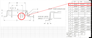
The question I have is: Why is there a gap/distance shown beween the bottom of the device and the bottom of the leads, indicated by symbol "A"? As the device has a thermal pad, I would expect "A" to be zero. Is this gap required to account for the solder paste thickness?

Many thanks and best regards, 

Jeroen

  • Hi Jeroen,

    Unfortunately, I do not have a definitive answer to your question.  However, I believe that you provided a good explanation as to why there is a gap.  Another factor that might contribute to this gap could be lead forming tolerances.  If there is tolerance in the lead height relative to the thermal pad, it would be important to ensure that the leads sit far enough "below" the thermal pad in order to make good contact with the board.  This could be accomplished by leaving a small height difference between the leads and thermal pad in order to ensure that leads make good contact with the PCB.

    Thanks,

    Drew