This thread has been locked.

If you have a related question, please click the "Ask a related question" button in the top right corner. The newly created question will be automatically linked to this question.

TCA9509: IoL question

Part Number: TCA9509
Other Parts Discussed in Thread: TMP100, , TCA9517

Dear team,

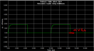
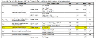
According to datasheet, maximum IoL(Low-level output current) level is 6mA.

My question is, Is there any side effect if the current is higher than 6mA?

I think output voltage level may not be as low as 0V in this application. please let me know if there are any side effect. Thanks.

Regards,

Ben

  • Hi Ben,

    The IOL current is directly tied to your VOL voltage. A higher VOL would mean that there is less of a voltage drop from your VCC pull up voltage and therefore you would have less current. The stronger your current the lower your VOL is. In the real world your VOL will never actually be at 0V. The mosfets within these devices have an RON resistance that creates a voltage divider with your pull up resistor. Since the RON resistance will never be 0 your voltage level will never be at exactly 0V.

    For this device we specify that at an IOL of 6mA for the B side you can expect to see a VOL of 0.2V maximum:

    You have to make sure that the device on the B side can accept a VOL voltage of 0.2V. That means that you have to check that the VIL of the device on the B side is greater than 0.2V. You can see the same thing is laid out for the A side. But keep in mind that the A side has a static voltage offset and it has it's own current source. So you should not place any pull up resistors on the A side.

    Let me know if this makes sense, and if it answered your question don't forge to hit the green button on my post.

    Best,

    Chris

  • Hi Chris,

    thank for your reply

    but I have some question below to "You have to make sure that the device on the B side can accept a VOL voltage of 0.2V. That means that you have to check that the VIL of the device on the B side is greater than 0.2V. You can see the same thing is laid out for the A side. But keep in mind that the A side has a static voltage offset and it has it's own current source. So you should not place any pull up resistors on the A side."

    AS far as I understand the circuit should be like

    to my understand you said if Bside's VOL is lower than 0.2V,

    I can assume it is PASS

    Is the right?

    Thank you

    Tommy

  • Tommy,

    This device is essentially a pass through for two or more I2C devices to talk to each other. When I say "You have to make sure that the device on the B side can accept a VOL voltage of 0.2V." I am talking about the device/devices that you would connect to the B side of this device. For instance lets say you have a temp sensor like the TMP100. If you go into the datasheet of this device you will see what value it's VIL is rated for. This is essentially the threshold for the device to read a valid logic low. 

    For the TMP100 the VIL threshold is 0.3*V+ which is your supply voltage. So if you apply 3.3V to V+ your VIL threshold would be 0.3*3.3=0.99. We know that for the TCA9509 on the B side if we size our pull up resistor such that the current going through our pin is 6mA we will be able to achieve a VOL of 0.2V at most. Since 0.2V is below our VIL threshold for the temp sensor on the B side then we know that these two devices are compatible. Keep in mind that on the B side you can change your pull up resistor value and therefore change your current. A larger pull up resistor will give you a lower VOL and a smaller pull up resistor will give you a higher VOL.

    On the A side we have a static voltage offset on this device. This means that no matter what is attached to the A side the output low voltage of the A side will always be the static voltage offset. For the TCA9509 this is at most 0.3V. The problem with devices with a static voltage offset is that any devices on the static voltage offset side have to be able to drive an output low that is lower than the VILC of the device. So lets say our TMP100 was connect to the A side of the device. Well the VOL of the TCA9509 matches with the VIL of the TMP100. But we have to check if the VOL of the TMP100 matches with the VILC of the TCA9509. Depending on your voltage supply the VILC of the TCA9509 is as low as 0.05V. For the TMP100 it has a VOL of at most 0.4V with a IOL of 3mA. Now with most devices this means that you can increase your pull up resistor in order to decrease your current and create a lower VOL. But with the TCA9509 it supplies it's own current for the A side of the device. This means that you can't attach pull up resistors to the A side of the device. Internally, the device has a 1mA current source so if your target device can't output a voltage lower than the VILC then you can't use the TCA9509.

    Another level shifter that may be easier for you to use is the TCA9517. This device still has a static voltage offset but it's VILC is much higher. It also allows for pull up resistors on both sides and will probably make it easier for you to design your system. If you are still interested in using the TCA9509 then let me know. The biggest takeaway here is that you have to make sure that all your VOLs match up with your VILs.

    Best,

    Chris

  • Hi Chris,

    thanks for you answer!

    that me clear the problem

    let me show the picture below

    for example:

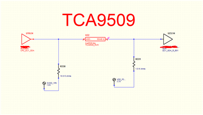
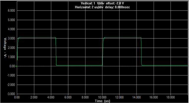
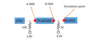
     here is the topology that I  simulated

      to Aside, it can meet the spec of VILc  


     to Bside, it can meet the spec of VOLB  

    the thing I worried about is although I meet the spec in VOLB (<0.2V)

    but the current IOL is bigger than spec 

    In cases where all voltages meet the spec, but cuttent is not.

    Does current lead to any phenomenon? like chip damage... or not.

    Thanks 

    Tommy

  • Tommy,

    To reiterate you should not be using a pull up resistor on the A side of the TCA9509.

    The scope shots you are showing are just simulations. The simulation is not going to give an accurate reading of the current and voltage low in a real world setting. It will just give you an estimation of what it could be. In fact this simulation could just have the output low of the TCA9509 B side to be 0.2V automatically. I am unsure if they simulated every single FET that is inside this device.

    What is the current you are measuring?

    Best,

    Chris

  • Hi Chris,

    simulations show current will be 10mV, but max allowable value is 6mA.

    Will I/O get burned or it will work?

    but current will be max out at 6mA on Bside.

  • TYPO (simulations show current will be 10mA)

  • Tommy,

    6 mA is not the maximum current that this device can source. It has a maximum output clamp current of -20mA. so any current above this will damage the device. 10 mA is fine but once again this is a simulation so I can't say accurate this will be to real life. Eitherway, as long as you remove the pull up on the A side your schematic looks good and it should work.

    Best,

    Chris