This thread has been locked.

If you have a related question, please click the "Ask a related question" button in the top right corner. The newly created question will be automatically linked to this question.

XIO3130: Port not working - Debug

Part Number: XIO3130

Hi there,

Customer is having an issue with the XIO3130.


Here is the issue:


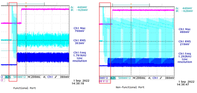
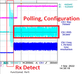
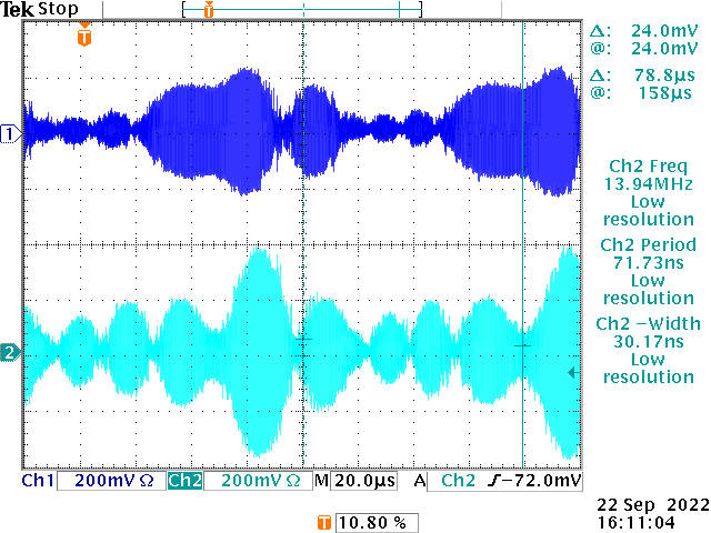
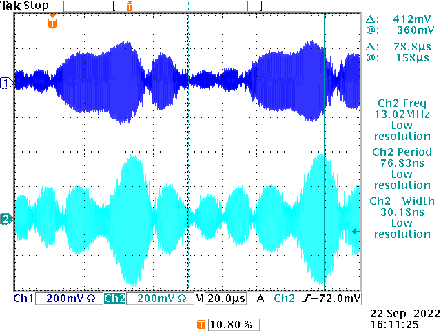
Although the device seems properly strapped, and devices are present on downstream ports 1 and 2, customer is only seeing activity on downstream port 2.

If they scan the PCI bus, they see the device itself, all its downstream ports, as well as the device on downstream port 2, but nothing on downstream port 1 (no reference clock is present – see below)

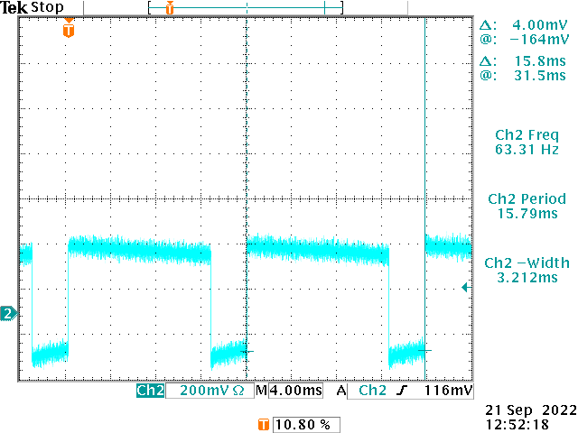
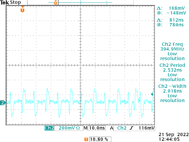
Even though downstream port 3 is not enabled, there is a reference clock present (100Mhz – see below)


Here is a little more detail:
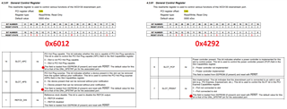
 

DN1_DPSTRAP = 3.3V

GPIO[0] = 418 mV (4.7K Resistor)

GPIO[1] = 0V

GPIO[2] = 3.3V

DN1_REFCLKO: No activity


DN2_DPSTRAP = 3.3V

GPIO[4] = 426 mV (4.7K Resistor)

GPIO[5] = 0V

GPIO[6] = 3.3V

DN2_REFCLKO: 100 MHz clock


DN3_DPSTRAP = 0V

GPIO[8] = 3.3V

DN3_REFCLKO: 100 MHz clock


Do you think somebody could help explain this behavior? Anything missed in the datasheet?

Thanks!

  • Hello,

    So the question is, why isn't DN1_REFCLK0 outputting a reference clock?  Is it possible to swap the device on Port 1 and the device on Port 2 to see if this is device-related?  It could be that one of the devices is in a low-power state and is not requesting a reference clock.

    Thanks,

    Nicholaus

  • Unfortunately, this is not a slot-based application - it is not possible for us to switch the ports the devices are on.

    The EEPROM contents were initially unprogrammed. We thought this might have a bearing on the issue. We subsequently programmed the contents of the EEPROM with the following contents:


     0  1  2  3  4  5  6  7  8  9  A  B  C  D  E  F

    0x00

    0x10

    0x20

    0x30

    0x40

    0x50

    4C 00 24 00 00 00 00 00 00 00 00 00 80 46 00 00

    00 00 00 00 00 00 00 00 00 14 32 02 00 00 00 00

    78 56 34 12 02 24 3F 04 01 00 01 00 00 00 00 14

    32 90 00 1A 08 00 02 00 01 00 00 00 00 14 32 90

    00 1A 10 00 02 00 01 00 00 00 00 14 32 90 00 1A

    18 00

    The data was read by the switch upon power-on (verified with a logic analyzer). This did not change the behavior - the device on Port 1 is still not visible behind the switch.

    I'm not sure I understand the reference to downstream devices not requesting a reference clock - there are no interface signals of this sort on the device. Each port has a PCIe TX lane, RX lane, and DNx_DPSTRP (enable) and RST pins. The DNx_DPSTRP pins are strapped by default to enable ports 1 and 2 (and disable Port 3), and the RST pins are outputs and should have no effect on the problem.

    What curious is that although Port 3 is disabled, there is activity on the DN3_REFCLKO signals.

  • A bit more information:

    Dumping the PCI Config Space of the 3 downstream ports may provide a clue as to the problem:

    Port 1 Register 0x9A reports a "Correctable Error Detected", but I do not have the details of the error source.

    I can provide the contents of the register dump if it would be helpful (I am trying not to overload the thread with information Slight smile)...

  • Hi Steven,

    Sorry, I expected CLKREQ#, but it's possible the CLKREQ# wasn't included in the PCIe Gen1 specification.

     A correctable error is correctable by the PCIe hardware by definition, so I don't expect that to cause a failure.  Having said that, it would still be helpful to have a register dump of the PCI config space and see if there are any clues to what is going on.  I will review the data provided and get back to you ASAP.

    Regards,

    Nicholaus

  • Nicholaus,

    Thanks very much for getting back to me so promptly. Here is the dump you so graciously asked for, along with some annotations. I would also appreciate your feedback on the EEPROM contents I provided in my previous response - I note that there is at least one divergence from the "TI Proprietary Register" contents contained in Table 3-3 of the device datasheet. The difference comes from our use of the contents of the EEPROM provided on your evaluation board, on which all 3 downstream ports were functional.

    Bus #3 Devices (XIO3130 Downstream ports)

    REGISTER         Device 0       Device 1       Device 2

                     (Port 1)       (Port 2)       (Port 3)

    ===========     ==========     ==========     ==========

    DEVID           0x8233104C     0x8233104C     0x8233104C

    DEVCTRL         0x00100406     0x00100407     0x00100404

    CLASS           0x06040002     0x06040002     0x06040002

    HEADER          0x00010010     0x00010010     0x00010010

    TERMBASE1       0x00000000     0x00000000     0x00000000

    TERMBASE2       0x00000000     0x00000000     0x00000000

    BUS_DEF         0x00040403     0x00050503     0x00060603

    IO_BASE         0x000001F1     0x00001111     0x000001F1

    MEM_BASE        0x0000FFF0     0xD100D100     0x0000FFF0

    PRE_BASE        0x40114001     0x40314021     0x0001FFF1

    PREBASEUP       0x00000000     0x00000000     0x00000000

    PRELIMUP        0x00000000     0x00000000     0x00000000

    IOBASEUP        0x00000000     0x00000000     0x00000000

    CAP_PTR         0x00000050     0x00000050     0x00000050

    PCI_38h         0x00000000     0x00000000     0x00000000

    INTCTRL         0x0003010B     0x0003010C     0x0003010E

    PCI_40h         0x00000000     0x00000000     0x00000000

    PCI_44h         0x00000000     0x00000000     0x00000000

    PCI_48h         0x00000000     0x00000000     0x00000000

    PCI_4ch         0x00000000     0x00000000     0x00000000

    CAP_PPMI        0xFE437001     0xFE437001     0xFE437001

    PM_CSR          0x00000008     0x00000008     0x0000010B

    PCI_58h         0x00000000     0x00000000     0x00000000

    PCI_5ch         0x00000000     0x00000000     0x00000000

    PCI_60h         0x00000000     0x00000000     0x00000000

    PCI_64h         0x00000000     0x00000000     0x00000000

    PCI_68h         0x00000000     0x00000000     0x00000000

    PCI_6ch         0x00000000     0x00000000     0x00000000

    CAP_MSI         0x00818005     0x00818005     0x00818005

    MSI_ADDRL       0xFEE01004     0xFEE01004     0xFEE01004

    MSI_ADDRH       0x00000000     0x00000000     0x00000000

    MSI_DATA        0x00004029     0x0000402A     0x0000402B 0x7C

    CAP_SubSysID    0x0000900D     0x0000900D     0x0000900D 0x80

    CAP_SUBID       0x00000000     0x00000000     0x00000000

    PCI_88h         0x00000000     0x00000000     0x00000000 0x88

    PCI_8ch         0x00000000     0x00000000     0x00000000 0x8C

    PX_CAP          0x01610010     0x01610010     0x00610010 0x90  Ports 1 and 2 are "Implemented"

    PX_DEVCAP       0x00008001     0x00008001     0x00008001 0x94

    PX_DEVCTL_STS   0x00112000     0x00102000     0x00102000 0x98  Port 1: "Correctable Error Detected"

    PX_LINKCAP      0x011E4C11     0x021E4C11     0x031E4C11 0x9C  Port Numbers defined: 1, 2, 3

    PX_LINKCTL_STS  0x10010140     0x30110140     0x10010140 0xA0  ???

    PX_SLOT_CAP     0x00000042     0x00000042     0x00000000 0xA4

    PX_SLOT_CTL     0x015803C0     0x015803C0     0x005803C0 0xA8

    PXRootCTL       0x00000000     0x00000000     0x00000000 0xAC

    PxRootStatus    0x00000000     0x00000000     0x00000000 0xB0

    PCI_B4h         0x00000000     0x00000000     0x00000000

    PCI_B8h         0x00000000     0x00000000     0x00000000

    PCI_Bch         0x00000000     0x00000000     0x00000000

    PCI_C0h         0x00000000     0x00000000     0x00000000

    PCI_C4h         0x00000000     0x00000000     0x00000000

    PCI_C8h         0x03000001     0x03080001     0x03100001 TI Prop

    PCI_Cch         0x00000000     0x00000000     0x00000000 TI Prop

    PCI_D0h         0x32140000     0x32140000     0x32140000 TI Prop

    PCI_D4h         0x00004292     0x00004290     0x00000011 General Control

    PCI_D8h         0x00000000     0x00000000     0x00000000 TI RSVD

    PCI_Dch         0x00000000     0x00000000     0x00000000 TI RSVD

    PCI_E0h         0x00000000     0x00000000     0x00000000 TI RSVD

    PCI_E4h         0x00000000     0x00000000     0x00000000 TI RSVD

    PCI_E8h         0x00000000     0x00000000     0x00000000 TI RSVD

    PCI_Ech         0x0000001A     0x0000001A     0x0000001A 0xEC

    PCI_F0h         0x00000000     0x00000000     0x00000000 TI RSVD

    PCI_F4h         0x00000000     0x00000000     0x00000000 TI RSVD

    PCI_F8h         0x00000000     0x00000000     0x00000000 TI RSVD

    PCI_Fch         0x00000000     0x00000000     0x00000000 TI RSVD

    PXAdvErrReport  0x00010001     0x00010001     0x00010001

    UncorrErrStat   0x00000000     0x00000000     0x00000000

    UnErrMask       0x00000000     0x00000000     0x00000000

    UnErrSevere     0x00062030     0x00062030     0x00062030

    corrErrorStat   0x00000000     0x00000000     0x00000000

    corrErrorMask   0x00002000     0x00002000     0x00002000

    AdvErrorCap     0x000000A0     0x000000A0     0x000000A0

    header1st       0x00000000     0x00000000     0x00000000

    header2nd       0x00000000     0x00000000     0x00000000

    header3rd       0x00000000     0x00000000     0x00000000

    header4th       0x00000000     0x00000000     0x00000000

    RootErrCmd      0x00000000     0x00000000     0x00000000

    RootErrStat     0x00000000     0x00000000     0x00000000

    ErrSrcId        0x00000000     0x00000000     0x00000000

  • Hi Steven,

    Thanks, I will review the data today and get back to you.

    Regards,

    Nicholaus

  • Hi Steven,

    I'm still looking, but I did find a useful post about this issue.  Maybe you can take a look and see if any of these situations apply to you: (+) XIO3130: Clock is not Generated in Down Stream Port - Interface forum - Interface - TI E2E support forums

    Do you think the issue mentioned regarding the downstream reset/in the errata is possible?  Also, do you happen to have multiple boards to see if all of them perform the same way?

    Regards,

    Nicholaus

  • Hi Steven,

    I have compiled the data provided (attached).XIO3130_Debug.xlsx

    Since you have said that this issue occurs whether the EEPROM was programmed or not, then I don't expect the EEPROM to be the issue.  Also, the configuration between Port 1 and Port 2 in the EEPROM is the same, so I would expect them to behave the same.   

    Could you provide a schematic of your board?  I have sent you a friend request so you can share it privately.

    Regards,

    Nicholaus

  • Hi Nicholaus,

    How can I share this privately?

    Note: The proposed implementation was already shared with TI when doing the initial design and no specific comments were made. However, I can prepare the information for you - I just need to know how to actually share the information...

  • Nicholaus,

    Here is more detailed comparison between our implementation and the EVAL board (schematics cover page date August 15th, 2007):

    Differences between XIO3130 Eval Board and Internal PCB

    1. DN1_REFCLKOp/n, DN2_REFCLKOp/n
       - AC-coupling caps placed on lines after damping/pull-down resistors (Not present on EVAL)
         NOTE: Shorted on DN1_REFCLKOp/n as a test ==> No difference in behavior

    2. Pins P01, C04
       - Tied directly to GND (EVAL board uses 4.7KOhm pull-downs)

    3. REFR0/REFR1
       - 14.530KOhm on internal PCB vs 14.532KOhm on EVAL

    4. GPIO Strappings
       - DN1_DPSTRP, DN2_DPSTRP are pulled high
       - DN3_DPSTRP in pulled low
       - GPIO11-18 are unconnected (possibility of PD)

    5. Register differences (not an exhaustive list):
       a. TI Proprietary register at PCI address D4h
          - Spec says it should be 0000 0010h, we read 0000 4290h
       b. TI Proprietary register at PCI address DCh
          - Spec says it should be 0000 0002h, we read 0000 0000h
       c. Downstream Ports Link PM Latency Register (PCI Offset E8h)
          - Spec says default is 3F24h, we read 0000h
       d. Global Switch Control Register (PCI Offset EAh)
          - Spec says default is 0004h, we read 0000h

    There are very few differences between the implementations, from a hardware point of view, but some of the proprietary register differences cause me a bit of concern. Is it possible we may find an answer in those registers...? What about the unused GPIO registers - Could one of them be having an effect on Port 1's functionality?

    Thanks,

    Steve

  • Hi Steve,

    I am still investigating the issue.  I have not found any information on the reserved registers so far, and I don't expect the GPIO registers having an effect on Port 1 as stated in the "GPIO Control and Data Registers (PCI offsets BCh, BEh, C0h, C2h, and C4h)" section of the Implementation guide.  This is assuming that the DNx_DPSTRPs are the same between the Internal Board and Eval board, but you have listed these as being different.  Is that true?

       - DN1_DPSTRP, DN2_DPSTRP are pulled high
       - DN3_DPSTRP in pulled low

    Attached is a summary of the issue.  Please let me know if any of the following points are not true:

    - Register settings are exactly the same between Port 1 and Port 2
    - Pin settings are exactly the same between Port 1 and Port 2
    - GPIO for port 1 and port 2 are exactly the same.  DNx_DPSTRAP is same for both, so GPIO is set set to hot-plug function
    - Failure is consistent across multiple boards
    - XIO3130 Eval Board and end-device eval board work well together
    - XIO3130 Eval Board EEPROM is the same as the internal board EEPROM
    - Port 1 generates what looks like a compliance pattern and does not complete link training.  Port 2 works well.

    Is it possible that the EEPROM is not being loaded?  I see from the data you shared that the EEPROM sets 0xEA to 0x04.  Is the upstream subsystem access register (0xE0) match what is set in the EEPROM ?

    Regards,

    Nicholaus

  • Nicholaus,

    I agree that I would not expect the GPIO programming to have an effect based on the notes included in the table, however I just wanted to make certain. I would like to clarify this comment: You refer to an Implementation Guide - Is this a section in the device datasheet or a separate document? I do not have a document called Implementation Guide, though I do have a "Design Guidelines for XIO3130" document (SLLA295A). Is this what you are referring to?

    I confirm each of your points as follows:

    - By Register settings I assume you mean Config Space, and no, they are not the same between Ports 1 and 2. The following is a list of the differences only between Ports 1 and 2. The other registers are programmed identically for Ports 1 and 2 (Port 3 has a few more registers programmed differently as it is disabled via strapping). I can provide a more comprehensive dump of registers, but limited this listing to only those registers that are different for brevity and ease of identification...

    Register         UpStream    Port 1      Port 2       Port 3
                                 (DN1)       (DN2)        (DN3)
    =============== ==========  ==========  ==========  ==========
    DEVCTRL         0x00100407  0x00100404  0x00100407  0x00100404 **** MEM/IO Disabled, MASTER_ENB = 1(?)
    BUS_DEF         0x00060302  0x00040403  0x00050503  0x00060603 **** Secondary/Subordinate buses = 4, 5, 6
    IO_BASE         0x00001111  0x000001F1  0x00001111  0x000001F1 ****
    MEM_BASE        0xD100D100  0x0000FFF0  0xD100D100  0x0000FFF0 ****
    INTCTRL         0x000300FF  0x0003010B  0x0003010C  0x0003010E **** Interrupt line = B, C, E
    PM_CSR          0x00000008  0x0000010B  0x00000008  0x0000010B **** PME_EN = 1; PWR_STATE = D3(hot)

    CAP_SUBID       0x3130102B  0x3130102B  0x3130102B  0x3130102B
    PX_LINKCAP      0x00064411  0x011E4C11  0x021E4C11  0x031E4C11 **** Port # = 1, 2, 3
    PX_LINKCTL_STS  0x10110040  0x10010140  0x30110140  0x10010140 **** Neg Link = 0; DLL_ACTV = 0 (DLL_LARC=1) <--+
    PX_SLOT_CTL     0x00000000  0x005803C0  0x015803C0  0x005803C0 **** DLLSC = 1 <--+
    PCI_C8h         0x02000001  0x03000001  0x03080001  0x03100001 **** Bit19 = 0 (Proprietary)

    - By Pin Settings I take you to mean the external strappings on the DNx_DPSTRAP and GPIO[0:2], GPIO[4:6] pins. Yes, they are identical.

    - Failure is consistent across multiple boards.

    - Downstream device eval board functions correctly in XIO3130 eval board.

    - EEPROM contents are not identical to EVAL board EEPROM: Some values do not correspond to specification requirements. The following table provides a comparison of the values suggested by the datasheet, those on the EVAL board, and those on our internal board (Differences are highlighted in orange):

    EEPROM Byte Address (hex)

    Programmed Values (hex)


    CONFIG Register Address (hex)

    Register Description


    Suggested

    Eval EEPROM

    Internal


    0

    4C

    4C

    4C

    NA

    Global Switch/Upstream Port Function Indicator(1)

    1

    0

    0

    0

    NA

    TI Proprietary register(1)

    2

    24

    24

    24

    0B4

    Upstream Port Link PM Latency register

    3

    0

    0

    0

    0B5

    Upstream Port Link PM Latency register

    4

    0

    0

    0

    0B8

    Global Chip Control register

    5

    0

    0

    0

    0B9

    Global Chip Control register

    6

    0

    0

    0

    0BA

    Global Chip Control register

    7

    0

    0

    0

    0BB

    Global Chip Control register

    8

    0

    0

    0

    0BC

    GPIOA register

    9

    0

    0

    0

    0BD

    GPIOA register

    0A

    0

    0

    0

    0BE

    GPIOB register

    0B

    0

    0

    0

    0BF

    GPIOB register

    0C

    0

    80

    0

    0C0

    GPIOC register

    0D

    0

    46

    0

    0C1

    GPIOC register

    0E

    0

    0

    0

    0C2

    GPIOD register

    0F

    0

    0

    0

    0C3

    GPIOD register

    10

    0

    0

    0

    0C4

    GPIO Data register

    11

    0

    0

    0

    0C5

    GPIO Data register

    12

    0

    0

    0

    0C6

    GPIO Data register

    13

    0

    0

    0

    0C7

    GPIO Data register

    14

    01

    01

    01

    0C8

    TI Proprietary register(1)

    15

    0

    0

    0

    0CC

    TI Proprietary register(1)

    16

    0

    0

    0

    0CD

    TI Proprietary register(1)

    17

    0

    0

    0

    0D0

    TI Proprietary register(1)

    18

    0

    0

    0

    0D1

    TI Proprietary register(1)

    19

    14

    14

    14

    0D2

    TI Proprietary register(1)

    1A

    32

    32

    32

    0D3

    TI Proprietary register(1)

    1B

    2

    2

    2

    0DC

    TI Proprietary register(1)

    1C

    0

    0

    0

    0DE

    TI Proprietary register(1)

    1D

    0

    0

    0

    0DF

    TI Proprietary register(1)

    1E

    0

    0

    0

    NA

    Global Switch/Upstream Port 0 Function Indicator

    1F

    0

    0

    0

    NA

    Not used

    20

    XX

    78

    2B

    0E0

    Subsystem Access Vendor ID register

    21

    XX

    56

    10

    0E1

    Subsystem Access Vendor ID register

    22

    XX

    34

    30

    0E2

    Subsystem Access Subsys ID register

    23

    XX

    12

    31

    0E3

    Subsystem Access Subsys ID register

    24

    0

    2

    2

    0E4

    General Control register (2h to disable L1)

    25

    24

    24

    24

    0E8

    Downstream Port Link PM Latency register

    26

    3F

    3F

    3F

    0E9

    Downstream Port Link PM Latency register

    27

    4

    4

    4

    0EA

    Global Switch Control register

    28

    1

    1

    1

    NA

    Downstream Port 1 Function Indicator

    29

    0

    0

    0

    NA

    Not used

    2A

    01

    01

    01

    0C8

    TI Proprietary register(1)

    2B

    0

    0

    0

    0CC

    TI Proprietary register(1)

    2C

    0

    0

    0

    0CD

    TI Proprietary register(1)

    2D

    0

    0

    0

    0D0

    TI Proprietary register(1)

    2E

    0

    0

    0

    0D1

    TI Proprietary register(1)

    2F

    14

    14

    14

    0D2

    TI Proprietary register(1)

    30

    32

    32

    32

    0D3

    TI Proprietary register(1)

    31

    10

    90

    10

    0D4

    General Control register

    32

    60

    00

    60

    0D5

    General Control register

    33

    1A

    1A

    1A

    0EC

    L0s Timeout register

    34

    0

    08

    0

    0EE

    General Slot Info register

    35

    0

    0

    0

    0EF

    General Slot Info register

    36

    2

    2

    2

    NA

    Downstream Port 2 Function Indicator

    37

    0

    0

    0

    NA

    Not used

    38

    01

    01

    01

    0C8

    TI Proprietary register(1)

    39

    0

    0

    0

    0CC

    TI Proprietary register(1)

    3A

    0

    0

    0

    0CD

    TI Proprietary register(1)

    3B

    0

    0

    0

    0D0

    TI Proprietary register(1)

    3C

    0

    0

    0

    0D1

    TI Proprietary register(1)

    3D

    14

    14

    14

    0D2

    TI Proprietary register(1)

    3E

    32

    32

    32

    0D3

    TI Proprietary register(1)

    3F

    10

    90

    10

    0D4

    General Control register

    40

    60

    0

    60

    0D5

    General Control register

    41

    1A

    1A

    1A

    0EC

    L0s Timeout register

    42

    0

    10

    0

    0EE

    General Slot Info register

    43

    0

    0

    0

    0EF

    General Slot Info register

    44

    2

    2

    2

    NA

    Downstream Port 3 Function Indicator

    45

    0

    0

    0

    NA

    Not used

    46

    01

    01

    01

    0C8

    TI Proprietary register(1)

    47

    0

    0

    0

    0CC

    TI Proprietary register(1)

    48

    0

    0

    0

    0CD

    TI Proprietary register(1)

    49

    0

    0

    0

    0D0

    TI Proprietary register(1)

    4A

    0

    0

    0

    0D1

    TI Proprietary register(1)

    4B

    14

    14

    14

    0D2

    TI Proprietary register(1)

    4C

    32

    32

    32

    0D3

    TI Proprietary register(1)

    4D

    10

    90

    10

    0D4

    General Control register

    4E

    60

    0

    60

    0D5

    General Control register

    4F

    1A

    1A

    1A

    0EC

    L0s Timeout register

    50

    0

    18

    0

    0EE

    General Slot Info register

    51

    0

    0

    0

    0EF

    General Slot Info register

    - Port 1 seems to generate a permanent stream of clocks on the PET lines. Exactly what the pattern correspond to is hard to say... Port 2 functions properly - the downstream device responds and can be accessed.

    - It is unlikely the data is not being loaded. I have previously take a logic analyzer trace illustrating the device's being loaded, and the register dump above includes the SubSysID register, which contains the data provided in the EEPROM.

    If there is anything else you would like to confirm, please let me know.

    Regards,

    Steve

  • Hi Steve,

    I see.  Thanks for the clarifications.   It looks like all of the settings are the datasheet-recommended values except for the disabling of L1, and the EERPOM is probably not the issue due to the fact that Port 1 and Port 2 have identical EEPROM settings.

    The implementation guide is available through the XIO3130 product page, I'm not sure why the titles are different but they are the same document (SLLA295A) XIO3130 Implementation Guide (Rev. A).  

    Regards,

    Nicholaus

  • Hi Nicholaus,

    I do have the document - the file name did not reflect the actual title of the document itself... Did not find anything particularly helpful (to my problem, that is) there anyway... 

    I have a couple of questions for you regarding voltage levels and pin definitions:


    If you go all the way back up to the 1st post on this thread, you'll see that I provided the voltage levels measured on several of the pins used as Hot Plug pins for the downstream ports. Specifically, GPIO[0] and GPIO[4] for Ports 1 and 2, respectively. The levels measured were approximately 420 mV (on each pin), which isn't really problematic given the Vil of the GPIO pins, but I'm wondering if it's normal, given the pins are supposedly in input mode and there's a reasonable pull-down resistor on each pin (4.7KOhm). I would have expected a lower voltage than this, and I'm just wondering if it's perhaps a sign of something else going on with the device.

    The other thing I'd like to confirm is that the pins GPIO[1] and GPIO[5], which serve as PowerOn# pins for their respective downstream ports, are actually output pins. I've currently got pull-downs on these pins, but I don't think their actually necessary, and may in fact be masking what is happening...

    Thanks for your feedback,

    Steve

  • Hi Steve,

    I also thought this voltage is a bit high.  I'm unable to measure this on the EVM since it does not have a pulldown resistor populated.  However, I do agree with you that it would be good to remove the pulldown on the PWRON# pin in order to check its value without it.  

    GPIO[0] and GPIO[4] are the PRSNT# pins: A PCI Hot Plug card or device is attached to a port when this signal is low.  This signal is reported in the PDC bit of the Slot Status register. When this signal is in a de-asserted high state, the DNn_PERST pin is asserted low, REFCLK is disabled, and PWRONn is de-asserted high.

    We can confirm the value of PRSNT# in the PCI config space in register 0xAA.  

    Port 1 (PX_SLOT_CTL)
    Slot Status:   0xAA = 0x0058
    Slot Control:  0xA8 = 0x03C0

    Port 2 (PX_SLOT_CTL)
    Slot Status:   0xAA = 0x0158, 0b0000000101011000 (DLLSC shows Data Link Layer Status changed on only port 2, PDC bit of Slot Status register shows PDS "changed", PDS bit is set to 1 or presence detected)
    Slot Control:  0xA8 = 0x03C0

    It shows that the value is registered as low from the PRSNT# pin.  It's a little bit curious that PDS bit has "changed" considering it should always be present due to the pulldown.

    I'm wondering if PRSNT# has any transients that could cause issues for Port 1.  One thing that may help circumvent this issue is to set SLOT_PRSNT in the General Control register = 0 through EEPROM, that way the PDS bit is always always asserted.  As I recall you do not have slots in your design, so this is the appropriate value in any case.  

    By the way, does the PCI_D4h general control register in the PCI Config space match for Port 1 and Port 2 after you made the modification to the crystal on the Port 2 device?  

    Regards,

    Nicholaus

  • Hi Steve,

    I have found the reserved register document, and the 0xC8h register is the only one in your previous data I see that is different between Port 1 and Port 2, it contains a captured bus/device number and unfortunately doesn't tell us anything significant.

    Regards,

    Nicholaus

  • Hi Steve,

    I'm wondering if the Port 2 oscilloscope screenshot that you shared that looks like a clock pattern is actually the XIO3130's Rx Detection pulses, and the XIO is not detecting a valid termination by the end-device.  Is there any way to confirm that the the end-device Rx on Port 2 is terminated in 50ohms (100-ohm differential)?    

    In the Port 1 Tx this pattern goes away; this may be because the 50-ohm Rx was detected and it has moved into the Polling state.

    I will see if I can get the XIO3130 to produce Rx detection pulses in the lab to compare with yours.

    Regards,

    Nicholaus

  • Hi Nicholaus,

    Just so we're clear: Port 2 is the functional port - it's Port 1 that is non-functional. The REFCLKO's on both ports are terminated to 50 Ohms according to the device datasheet and eval board schematics.

    The TX lines on Port 1 never seem to exist the initial polling state. See following image: Functional Port = Port 2; Non-functional Port = Port 1

    Regards,

    Steve

  • Hi Steve,

    Sorry for the mix up. I am asking if the TX lines, not REFCLK, is terminated in 50ohms (100 ohm differential) by the end device.  It it's possible the end-device may have it's pins in a high-Z state or is marginal.

    The initial state for a PCIe device is Rx Detect.  It sends pulses out of the Tx lines to detect if there is a valid 50 ohm termination.  If there is, then it means there is a device connected and it will continue into the polling state.  When in polling the end device should respond with TS1/TS2 packets, if there is no TS1/TS2 packets detected after a certain amount of time, then it will go into compliance and should transmit something other than a clock pattern.  

    As you have said, what we see doesn't seem to be either polling or compliance.  So, my thought is that the XIO3130 Port 1 is actually stuck in detect and never makes it to polling because it cannot "see" the end device due to the lack of a 50ohm termination at the far-end Rx.

    Regards,

    Nicholaus

  • Hi Steve,

    Sorry for the long delay.  A couple of the XIO3130 EVM boards I was testing with were bad, so it took a while to get the data.  However, it does seem like there could be issues with the termination impedance on the PCIe Tx lanes coming from the XIO3130 on port 1; a 50ohm termination value should be provided by the Rx of the end device on port 1. Rx pulses on the Tx lines will look like a high-duty clock signal that repeats about every 14ms.  Here is an example from an XIO3130EVM in the lab.  

    Below is a scope shot you sent me.

    If there was a 50ohm termination at the far-end of the Tx lines, then this signal should not be visible.  PCIe devices often have the ability to switch between high-Z and 50ohm.  Can you confirm that the impedance seen at the Rx of the end device on port 1 is close to 50ohm and not high-Z?

    Regards,

    Nicholaus

  • Hi Nicholaus,

    Thanks very much for this information - the waveforms do look suspiciously similar.

    The PCIe traces for both ports are routed with the same characteristics - 100 Ohm differential termination. The PCB fab's report indicates the trace impedances are pretty much bang on, so if what you theorize is true, the downstream device is not properly configuring its' inputs.

    I will have to take a closer look at this with Intel. What I am having trouble understanding, though, are the following points:

    1. The 2nd port drives another Intel ePhy and there are no issues (the 2nd device automatically adjusts its' input impedance?)

    2. The same Intel ePhy is used on other boards with no issues. On the other boards they are driven directly by an Intel SoC.

    Why/How would the device be configured differently in each case?

    You pose a very interesting question, and I will have to take a closer look at this. I will get back to you as soon as I have any further information.

    Regards,

    Steve

  • Hi Steve,

    Some PCIe devices can disable/enable their Rx terminations.  For example, if a PCIe retimer doesn't detect 50ohms at it's Tx, then it's Rx for the corresponding lane will stay at high-Z until it does detect one.  There is a chance that the Intel ePhy is not enabling it's terminations for some reason.  The quickest way to find out is to measure or force the impedance on the board if possible.  If the XIO3130 Tx is terminated by 50ohms then we should see it go into polling, and then either compliance (no PCIe device present) or the link configuration state.  This is what I believe is happening on Port 2.  It may be helpful to zoom in and confirm this that the portion of the signal are Rx detect pulses from the XIO in the functional Port 2 case. 

    If the termination value at the Intel Rx is marginal, then detection would depend on the specific device's Rx detection design.  This means one PCIe device could work successfully, while the XIO3130 does not.  Although it's not common I have seen interop issues like this occur. This E2E post shows an example how Rx detection works.  

    (2) DS80PCI402 / about Auto RX-Detect - Interface forum - Interface - TI E2E support forums

    However, I don't think this is the case here because the oscilloscope shot that you showed me doesn't show "small" pulses, it shows large pulses that indicate a high impedance, not a marginal impedance.  If it were marginal the pulses would be barely visible.

    Regards,

    Nicholaus

  • Hi Nicholaus,

    Thanks for the detailed explanation and the references about the Auto RX-Detect mechanism: I'll take a closer look at them and increase my own knowledge at the same time!!! (There's an expression in French that essentially says "I'm going to go to sleep less stupid tonight" - that pretty much sums up my thoughts at the moment... Laughing)

    I'm currently trying to determine if Intel provides any way of configuring this termination value - I'm also going to try to solder 50 Ohm termination resistors to the pins in question (not going to be easy, but at least the package is not BGA device). It'll be a rough test, but if this is indeed the issue I should be able to at least prove it.

    I'll let you know what the results are.

    Regards,

    Steve

  • Nicholaus,

    I was able to solder terminations to the lines and they certainly changed the behavior of the signals, but did not change the actual result - the device is still not responsive.

    The following are images of the TX signals before/after the addition of the terminations:


    I do have a question for you regarding the XIO3130's detection mechanism: You state that the device detects the impedance on the signals and determines whether or not a device is present. What is the tolerance on that impedance? 50-Ohms +/- ?

  • Hi Steve,

    That impedance is defined by the PCIe specification as 40ohm minimum, 60ohm maximum.

    The next sequence should be polling, then the end-device should respond to the XIO3130 with TS1/TS2 packets, and then it should move into configuration and establishing a link.  

    If the end-device does not respond with TS1/TS2 packets, then the XIO3130 should move into compliance.  

    Here is a screenshot from the lab after I terminated the lines with 50 ohms.  Right now I only have my low-bandwidth scope, so I can't see the actual pattern yet, but this should be a compliance pattern.  I will confirm as soon as a high-speed scope becomes available.

    Regards,

    Nicholaus

  • Nicholaus,

    Just to be clear, do the two signals on your scope represent the +/- pair PET emanating from the XIO3130, or one of the PET signals and one of the PER signals?

    Thanks,

    Steve

  • Nicholaus,

    The following images appear to show the same thing as in your images, though there doesn't appear to be the same "synchronicity".

    (These are three images taken of the -/+ve PET signals AFTER the AC-coupling cap)


  • Hi Steve,

    Yes, if you terminate only one of the two PET pairs, then the XIO3130 will not advance to polling.  Both Tx+ and Tx- must be terminated.

    If there is a high-speed scope, I think I may be able to tell the difference between compliance and polling, but it's hard to say what's going on without it.  

    I think it may be good to circle back to what seems to be the issue in that the end-device is not enabling it's terminations for the XIO3130.  Forcing the termination using external 50 ohms may get us to compliance, but it may not cause the PCIe link to work.  Are there any tools we can use on the Intel PHY side to debug this issue?  Maybe there is a way to force the internal terminations to 50 ohms?

    Regards,

    Nicholaus

  • Nicholaus,

    Thanks for your response. To answer your question, I'm trying to get an answer from Intel regarding their device. A support ticket has been opened, but no feedback has been received. I have seen nothing in any documentation that refers to adjusting or tweaking the impedance of the ethernet controller's inputs. The design guidelines state that for Gen-1 applications, 100-Ohm differential routing is acceptable, though for Gen2/3 operation 85-Ohm is necessary.

    I also wanted to make clear that I have terminated both PET- and PET+ from the XIO3130 close to their endpoints (Intel Ethernet controller). I guess my question is also partly: "Should the PET-/+ signals from the Ethernet controller also be terminated close the XIO3130? My sense from our discussions is that this should not be necessary, but I would like to hear your opinion on this.

    I can see if I can manage to get a better trace using a higher-speed scope (we have availability issues on our side, as well). Would you prefer a true differential probe or would the individual +/- traces be acceptable...?

    Thanks,

    Steve

  • Hi Steve,

    The 50ohm terminations for PCIe devices are internal to the PCIe device, so there should be no external terminations necessary. The Intel PHY should be providing them; I'm not sure why it is not. Maybe there is some condition or pin state that isn't met that it is expecting.   It may be helpful to check the signaling another board if this hasn't already been done. 

    Individual +/- traces would be fine.  

    Regards,

    Nicholaus

  • Hi Steve,

    I will be out next week, so I have alerted my colleagues of this issue.  They should continue to provide support next week.

    Regards,

    Nicholaus

  • Hi Steve,

    I'm continuing our discussion over e-mail here:

    Question: "Is it possible to disable the internal terminations on the RX pins of the XIO3130 (making the inputs high-impedance). In this way, I could potentially try to use an external termination and see if that might make a difference."

    Unfortunately, there is no way to force the termination value.  The XIO3130 Rx termination value is controlled by state machine.  I’m assuming the Intel device is similar.  This is why I expect this external termination experiment may get us past Rx Detection, because the requirement to exit Rx Detect is simply the detection of 50 ohms, however, it may not establish a link afterwards unless other requirements are met.  For example, the XIO3130 Rx is in a high-Z state "...when no power is present or Fundamental Reset is asserted." according to the datasheet.   However, if a fundamental reset is asserted or there is no power then link training should not begin even when termination is forced to 50 ohms through an external resistor.  A similar situation may be the case for the Intel device.

    Is there any way you could provide the PCI Configuration Space of the Intel device?  Maybe that has some useful information.

    Another thing to investigate would be the Intel Tx lines and see what type of electrical behavior we see there.  

    Regards,

    Nicholaus

  • Hi Steve,

    Just checking in. Has there been any updates on this issue?

    Regards,

    Nicholaus

  • Hi Nicholaus,

    We think we just found the answer, but it's bringing up another question that I'm hoping you'll be able to clarify.

    It appears as though the REFCLK Disable bit is being set to '1' during the boot process, but we're not certain by whom. I've got my low-level software guy telling me there's a "0%" chance of the coreboot setting the bit, yet the bit is definitely set to '1' if I read the General Control Register at offset 0xD4. It's also NOT set on the eval board, which is running under Windows, so that further bolsters the idea that it's a low-level issue.

    What's more curious is that the corresponding bit on Port 0 is NOT being set (which explains why Port 0 is working fine). 

    To recap: We've seen this issue whether the EEPROM is initialized or not. Bit 1 is set to '1' on Port 1, but NOT on Port 0. The EEPROM contents are defined such that the bit should be initialized to '0' when the EEPROM is used.

    I've asked the low-level software guy to ensure there are no "hidden" accesses in the code that secretly set this non-standard register, but while this is being done, I'd like to get your feedback on the following:

    1. Any ideas (other than software) why is Port 1's bit set to '1' while Port 0's bit is properly initialized to '0'? (Again, we're looking at a software cause for this)

    2. Are there any errata that may affect the loading of the configuration bits on power-up?

    3. Is it possible the setting of that specific bit is dependent on more than one field?

    Any feedback you  have would be great - I'll let you know as soon as we've confirmed whether or not there is an access to the register in question...

    Thanks and regards,

    Steve

  • Hi Steve,

    It's great that progress has been made.  One question about this result.  Didn't we see the REFCLK output signal being generated in your oscilloscope shots after replacing the crystal in the downstream device?  That would mean the XIO3130 digital is saying that the REFCLK is disabled, but it's electrically not disabled.

    1.  Here are some thoughts:

    In General Control Register (0xD4), the REFCK_DIS (bit 1) bit is set to "1", which is the root of the problem.  After PERST# pulse it should be reset to 0 and EEPROM load also has it set to 0, so it is getting changed to "1" sometime after PERST#.  I reviewed your schematic again, and it looks like the downstream PERST# pins are pulled to ground, but I saw in your oscilloscope shots a PERST# signal, so I'm unsure which one is correct.  Could you let me know?

    The SLOT_PFIP (bit 6) field can be used to disable REFCLK during power fault.  This field is set to "0" so it shouldn't apply.

    The RC_PF_CTL (bit 15) field can be used to disable REFCLK during power fault.  This field is set to "0" so it shouldn't apply.

    In Table 5-2, there is a section describing PCIe hot-plug side-band signals that could disable REFCLK, like PRSNT# and PWRGD#.  This goes back to your original issue where the ports are set to:

    DN1_DPSTRP    = 1 (PCIe Hot-Plug Enabled)
    GPIO0/PRSNT#  = 0 (Card Present)
    GPIO1/PWERON# = 0 (XIO3130 Output)             
    GPIO2/PWRGD   = 1 (Power Good)
    DN1_REFCLKO: No activity

    DN2_DPSTRP    = 1
    GPIO4/PRSNT#  = 0
    GPIO5/PWERON# = 0              
    GPIO6/PWRGD   = 1
    DN2_REFCLKO: 100 MHz clock

    Thy only thing that I can see possibly disabling the REFCLK is if there is noise or transient on PRSNT#, PWRGD, or PERST# causing REFCLK to be disabled, but if they're stable then this should be fine.  We can take a look at these signals for Port 1 during link-up to make sure it aligns with the sequence listed in Section 5.2 of the datasheet. 

    2. There are no errata that is not listed in PCI Express Packet Switch Silicon Errata List (Rev. A) (ti.com)

    3.  It looks like that specific bit could be affected by the items listed in #1, but there is no indication is directly dependent on another field.

    Regards,

    Nicholaus

  • Hi Nicholaus,

    Some success to report, but we're still confused here:

    We've checked our code and haven't found any software accesses to the register at offset 0xD4. We've attempted to patch the issue by checking the bit's status, and if it's at '1', setting it back to '0'. We think this is a viable work-around (though it has only been tested on a few boards at this point), but it does not address the fundamental issue: Why is the 'Disable" bit in the General Control Register set to '1' in the first place?

    With regards to you first question: The PERST# signal rises shortly after power-on, and should remain static. This is a 3.3V signal, and threshold levels should preclude any "noise" from creating a false transition. There are actually both upstream and downstream PERST# signals, right? We have never observed any issues detecting/configuring the XIO3130, so it is unlikely the "upstream" reset that would be causing a problem. If it were, why would it only affect Port 0??

    We seem to have established a clear link between the General_Control_Register[1] bit ('disable') and our inability to detect the downstream device. What are the conditions under which this bit will be set to '1'?

    1. EEPROM contents setting bit to '1' (Offset 0x31 for Port 0).

    2. You mention sideband signals such as PRSNT# and PWRGD#, yet these are all pulled to static values and shouldn't pose a problem.

    3. You also mention fields such as SLOT_PFIP and RC_PF_CTL that seem to be set so as not to cause any problems.

    4. There must be something else that can set the bit 'disable' to '1'... We need to know what that is...

    As a side note: Even thought the third downstream port is disabled, its' own REFCLK bit is enabled... This is counterintuitive, since I would expect the REFCLK to be disabled if the downstream port itself is disabled... Could this potentially provide a clue?

    I would like to say we are confident that our solution addresses the problem 100%, but I don't think we can at the moment. I really need to understand the mechanism by which the bit 'disable' is being set to '1'.

    So, summing up, I would have to say that my 1 question for you is the following:

    What can cause the bit 'Disable" of General Control Register for Port 0 ONLY to be set to '1'????

    Thanks for your feedback.

    Regards,

    Steve

  • Hi Steve,

    It is a good question.  The previous post are the ideas that I had that would cause this with the information available.  With your new workaround can you identify when and how many times the REFCLK_DIS bit changes from a 0 to a 1?  Maybe that can give a clue. To clarify, the output REFCLK is being output on Port 0 as we saw in your oscilloscope images, despite the clock disable bit being set, correct?

    When I mentioned the PERST# signal I was referring to the downstream DNn_PERST# signal, which should go to the downstream device.  However, it is shown as pulled to ground in the schematic unless R3782 was populated.  I think the upstream PERST# is fine as you said.  

    Since PWRGD# is pulled high, this means the link training sequence should begin as described in section 5.2.3.1 "PCI Hot Plug Power-Up Cycle With No PWRGDn Feedback".  If this sequence is not followed, then that could disable the REFCLK.  Why this is only happening to Port 0 is a mystery as there are no discernable differences from the schematic, so my thoughts are this is an interop issue with the device on Port 0.  I will ask internally to see if anyone has the digital design of this part and can tell me what internal states might affect this bit.  I am out of office today, so I will follow up early next week.

    Regards,

    Nicholaus

  • Hi Nicholaus,

    Unfortunately, the the way the algorithm is implemented it's not possible to determine if the disable bit is activated multiple times. Essentially, the algorithm is the following:

    If GeneralControlRegister[1] == '1' then

    {

       Set GeneralControlRegister[1] = '0'

       While (NegotiatedLinkWidth == 0h && nbRetries < 1,000,000); // 1E6 Maximum retries allowed.

    }

    Return control to Coreboot

    The only thing I can say at this moment is that all boards (so far) that have been programmed with this algorithm seem to be good (have gotten to the stage where the linux O/S is loaded and all devices - including both ethernet ports - are functional). This indicates that there is only the initial setting of the bit to '1' which we need to concern ourselves with. We are continuing to program boards and will perform more detailed testing to evaluate the robustness of this work-around. As an aside, it appears to take on the order of 100K polling operations for the PCIe link to be trained and the field NegotiatedLinkWidth to be set.

    My concern is that since we don't understand why the bit is toggled in the first place, it could happen again under "normal" operation and cause problems.

    With regards to your question: I cannot be certain of the exact timing of the clock vs the setting of this bit - I don't currently have a way of correlating the setting of the bit with the actual stopping of the REFCLK oscillations. 

    With regards to your question regarding R3782: This resistor allows us to gate the Ethernet controller's RST# pin with the PERST# signal of the PCIe switch downstream port. As you saw from the schematic, the default is NOT to include the downstream port's PERST# signal, but to generate the ethernet controller's RST# using another signal, derived differently. The caveat here, though, is that the timing of the reset signal does not necessarily coincide with the REFCLK having been stable for a predefined amount of time:

    As you can see from the image above, the top signal is the "default" RST# generation for the i226 ethernet controller. The middle signal is the PERST# signal rom the downstream port. We do have the ability to route the DN1 PERST# signal to the i226 controller, however we have found this is does not seem to be necessary for the following reasons:

    1. Doing so had no effect on whether or not the data link trained properly.
    2. The work-around we have implemented works under the conditions shown above (i226 RST# generated by default mechanism).

    NOTE: The cease in REFCLK oscillations shown above appears to be due to the faulty i226 crystal oscillator, as discussed earlier. For the purposes of this discussion, the salient information is the generation of the RST# signal vis-à-vis the arrival/stability of the REFCLK.

    As far as the Disable bit is concerned, the waveform below suggests that the bit is set approximately 2.2 seconds after oscillations begin:

    Adding the RST# signal and running our modified coreboot, this is what we find:

    From this mage, we see that the REFCLK oscillation stop at about 2.4 seconds (after removal of RST#), but resume approximately 1 second later (presumable due to our work-around).

    I don't really know if all this information will help to narrow-down the cause of the bit-assertion, but it's the best I can give you in terms of externally-visible  information that may help track down the problem. If there is any other measurement that would help you isolate the problem, please let me know.

    I will look further into the Section 5.2 references to see if I can find anything pertinent. We can touch base again next week.

    Regards,

    Steve

  • Hi Steve,

    I am concerned about the PERST# timing since this can be an issue under normal circumstances as the PCIe specification requires the signal to de-assert after REFCLK is stable, and the XIO3130 errata that states that there is a known bug related to the timing as well; however, if it works and you are confident it does not cause any issues then it is OK.

    It seems like the PERST# timing wouldn't have an effect on the REFCLK disable bit in any case.  The response from the design team is "hardware doesn't automatically update this bit".  So, the EEPROM, the software, and the XIO3130 are not updating this bit.  I'm not sure where else this could come from.

    Regards,

    Nicholaus

  • Hi Nicholaus,

    Just to be clear: The reset signal above is the primary PERST# signal, whereas the downstream clock is associated with the downstream PERST# signal (which has the option of being generated by the XIO3130). Neither option (both have been tried) has shown any difference in behavior - In both cases the DIABLE bit is being set to '1' sometime early in the boot process (see above oscilloscope images)


    I would like to confirm your assertion: According to the design team, hardware does not change this bit (DISABLE) on its' own ... am I correctly interpreting that statement? Does this mean that it cannot (no physical electrical connectivity), or it does not (slight difference I'd like to clarify....)

    According to the datasheet, the hardware default (i.e. in the absence of an EEPROM) is that the bit defaults to '0'. We have tested this case (EEPROM contents programmed to 0xFF), and we see the problematic behavior (DISABLE bit set to '1' requiring re-programming).

    With the external EEPROM programmed (General Control Register[15:0] set to 0x6010, as shown in various examples), we again see the same behavior (DISABLE bit set to '1' requiring re-programming).

    This doesn't really leave us much in the way of alternatives. We are currently verifying the status of this bit as soon as the device is able to respond to PCIe accesses on the Host Interface (as soon as it is programmed). We are reading a '1', which cannot be explained by a software access, and based on your response, we don't understand how the bit is being set... 

    I know these questions have been asked before, but:

    1. "How is this bit being set to '1'???
    2. "Why only Port 0?"

    We need some options - Has the design team actually opened up the code and checked to see by what mechanisms the offending bit can be set to '1'?

    We are trying to examine the primary PCIe interface to see if we can detect an access that might be setting the bit to '1', but are hamstrung by our lack of flying probe which would allow us to analyze the protocol...

    I'll get back to you if we find anything else here that may be helpful. Please try to see if you can dig up any additional information on your side.

    Thanks for your help.

    Regards,

    Steve

  • Hi Steve,

    I think we can rule out the EEPROM, if I remember correctly both ports are programmed the same way.  If we see it on Port 0 we should see it on Port 1.  Also, as you pointed out you tried other options, and it does not change the result.  This is easily tested.

    So, it is likely either the software or the device itself.   The PCIe configuration space for the XIO3130 is housed within the XIO3130 based on my understanding, so there should be electrical connectivity; however, the digital state machine is what determines if the bit can be set.  I trust the design team's response, but I will follow up and make sure they are sure.

    Please make sure the software doesn't set bit 1, bit 6, or bit 15 in 0xD4 for the XIO3130. 

    Regards,

    Nicholaus

  • Hi Steve,

    Here are some questions from the design team that I answered.  I just want to double-check here and make sure they are accurate:

    Are they getting clock out but the bit is reading wrong or they aren't getting clock out on one of the ports. 
    They are getting clock out for about 2 seconds until the clock will stop, possibly due to this bit change.
    Is it stuck at fault that they cannot change.
    No, their current workaround is that they change the bit back to “0” before link training.
    Do they see this in more than one unit. 
    Yes

    Regards,

    Nicholaus

  • Hi Steve,

    A follow-up question is what other bits, if any, get set around 2 seconds after PERST# is issued in the software?

    Regards,

    Nicholaus

  • Hi Nicholaus,

    Your answers to the first three questions are absolutely correct.

    As far as your follow-up question: I'm not certain how I can answer this properly... It sounds as though what you need is a dump of the registers at the moment we detect the bit has been set to '1' (just before we implement our re-programming algorithm). Although I have already provided dumps of the registers (earlier in this thread) they have been once control has been transferred to the O/S, and therefore several registers have been re-programmed by the low-level kernel.

    Please confirm if this is what you are looking for: It will take a bit of work, but I believe I can get something for you within a day or so...

    Thanks for getting back to me with this...

    Regards,

    Steve

  • Hi Steve,

    I think the design team wants to check what other registers may have been changed from the software that may indirectly affect this bit.  They are firm in the stance that the XIO3130 cannot make this bit change without external interference from software or EEPROM.

    Is it possible to provide all the changes the software makes to the XIO3130 config space directly from the code?  If that's not possible then a register dump before and shortly after PERST# may help identify what the software is doing.   

    Regards,

    Nicholaus

  • Hi Nicholaus,

    I understand what the hardware design team is getting at. Unfortunately, it may not be possible to get them exactly what they are looking for.

    First off, I think we can agree that it is not possible to dump the PCIe Config Space before (Upstream) PERST# has been de-asserted. The Downstream PERST# signal is hardware-controlled, and we cannot modify the low-level firmware to keep the downstream port(s) reset until we are ready to release them (I'm not even certain this level of control is possible with the XIO3130's registers).

    With regards to providing the accesses done by the low-level firmware, it is not possible for us to determine (by analyzing the source code) what registers may or may not be written by the software. Given the rather generic nature of linux and the device-specific nature of many of the registers, it is hard to fathom the low-level drilling down and initializing a group of registers specific to any given device - specifically when PCIe switches are very well-defined within the PCI-Express architecture.

    (The above being said, we are attempting to jerry-rig a setup that will allow us to capture all accesses performed to the upstream port. We have not yet been successful in getting a proper capture, however, so I cannot provide you with any concrete information at this time. As soon as we get this information I will send it to you)

    The best I can give you right now are the following dumps from 3 units taken as early as possible in the boot cycle. I have the upstream port as well as the 2 implemented downstream ports: Device 03:00.0 is the non-functional (REFCLK_Disable = '1') port and device 03:01.0 is the functional port (this is connected to a second Ethernet controller. I've highlighted the register under discussion, so it is easy to see...

    Board 1:

    PCI: 02:00.0 configuration space dump:
       0000: 8232104C 00100000 06040002 000
       0010: 00000000 00000000 00FF0302 000
       0020: 00000000 00010001 00000000 000
       0030: 00000000 00000050 00000000 000
       0040: 00000000 00000000 00000000 000
       0050: FE037001 00000008 00000000 000
       0060: 00000000 00000000 00000000 000
       0070: 00808005 00000000 00000000 000
       0080: 0000900D 3130102B 00000000 000
       0090: 00510010 00008001 00192000 000
       00A0: 10110140 00000000 00000000 000
       00B0: 08A00000 00000024 00000001 000
       00C0: 00000000 0007FBCC 02000001 000
       00D0: 32140000 00000002 00000000 000
       00E0: 3130102B 00000002 00043F24 000
       00F0: 00000000 00000000 00000000 000

    PCI: 03:00.0 configuration space dump:
       0000: 8233104C 00100000 06040002 000
       0010: 00000000 00000000 00000006 000
       0020: 00000000 00010001 00000000 000
       0030: 00000000 00000050 00000000 000
       0040: 00000000 00000000 00000000 000
       0050: FE437001 00000008 00000000 000
       0060: 00000000 00000000 00000000 000
       0070: 00808005 00000000 00000000 000
       0080: 0000900D 3130102B 00000000 000
       0090: 00610010 00008FC1 00112000 011
       00A0: 10010140 00000060 015803C0 000
       00B0: 00000000 00000000 00000000 000
       00C0: 00000000 00000000 06000001 000
       00D0: 32140000 00006012 00000000 000
       00E0: 00000000 00000000 00000000 000
       00F0: 00000000 00000000 00000000 000

    PCI: 03:01.0 configuration space dump:
       0000: 8233104C 00100000 06040002 000
       0010: 00000000 00000000 00000000 000
       0020: 00000000 00010001 00000000 000
       0030: 00000000 00000050 00000000 000
       0040: 00000000 00000000 00000000 000
       0050: FE437001 00000008 00000000 000
       0060: 00000000 00000000 00000000 000
       0070: 00808005 00000000 00000000 000
       0080: 0000900D 3130102B 00000000 000
       0090: 00610010 00008FC1 00102000 021
       00A0: 30110140 00000060 015803C0 000
       00B0: 00000000 00000000 00000000 000
       00C0: 00000000 00000000 00080001 000
       00D0: 32140000 00006010 00000000 000
       00E0: 00000000 00000000 00000000 000
       00F0: 00000000 00000000 00000000 000

    Board 2:

    PCI: 02:00.0 configuration space dump:
       0000: 8232104C 00100000 06040002 000
       0010: 00000000 00000000 00FF0302 000
       0020: 00000000 00010001 00000000 000
       0030: 00000000 00000050 00000000 000
       0040: 00000000 00000000 00000000 000
       0050: FE037001 00000008 00000000 000
       0060: 00000000 00000000 00000000 000
       0070: 00808005 00000000 00000000 000
       0080: 0000900D 00000000 00000000 000
       0090: 00510010 00008001 00192000 000
       00A0: 10110140 00000000 00000000 000
       00B0: 08A00000 00000024 00000001 000
       00C0: 00000000 0007FBCC 02000001 000
       00D0: 32140000 00000002 00000000 000
       00E0: 00000000 00000000 00040024 000
       00F0: 00000000 00000000 00000000 000

    PCI: 03:00.0 configuration space dump:
       0000: 8233104C 00100000 06040002 000
       0010: 00000000 00000000 00000006 000
       0020: 00000000 00010001 00000000 000
       0030: 00000000 00000050 00000000 000
       0040: 00000000 00000000 00000000 000
       0050: FE437001 00000008 00000000 000
       0060: 00000000 00000000 00000000 000
       0070: 00808005 00000000 00000000 000
       0080: 0000900D 00000000 00000000 000
       0090: 01610010 00008001 00112000 011
       00A0: 10010140 00000042 015803C0 000
       00B0: 00000000 00000000 00000000 000
       00C0: 00000000 00000000 06000001 000
       00D0: 32140000 00004292 00000000 000
       00E0: 00000000 00000000 00000000 000
       00F0: 00000000 00000000 00000000 000

    PCI: 03:01.0 configuration space dump:
       0000: 8233104C 00100000 06040002 000
       0010: 00000000 00000000 00000000 000
       0020: 00000000 00010001 00000000 000
       0030: 00000000 00000050 00000000 000
       0040: 00000000 00000000 00000000 000
       0050: FE437001 00000008 00000000 000
       0060: 00000000 00000000 00000000 000
       0070: 00808005 00000000 00000000 000
       0080: 0000900D 00000000 00000000 000
       0090: 01610010 00008001 00102000 021
       00A0: 30110140 00000042 015803C0 000
       00B0: 00000000 00000000 00000000 000
       00C0: 00000000 00000000 00080001 000
       00D0: 32140000 00004290 00000000 000
       00E0: 00000000 00000000 00000000 000
       00F0: 00000000 00000000 00000000 000

    Board 3:

    PCI: 02:00.0 configuration space dump:
       0000: 8232104C 00100000 06040002 00010000
       0010: 00000000 00000000 00FF0302 00000101
       0020: 00000000 00010001 00000000 00000000
       0030: 00000000 00000050 00000000 000000FF
       0040: 00000000 00000000 00000000 00000000
       0050: FE037001 00000008 00000000 00000000
       0060: 00000000 00000000 00000000 00000000
       0070: 00808005 00000000 00000000 00000000
       0080: 0000900D 3130102B 00000000 00000000
       0090: 00510010 00008001 00192000 00064411
       00A0: 10110140 00000000 00000000 00000000
       00B0: 08A00000 00000024 00000001 00000000
       00C0: 00000000 0007FBCC 02000001 00000000
       00D0: 32140000 00000002 00000000 00000002
       00E0: 3130102B 00000002 00043F24 00000000
       00F0: 00000000 00000000 00000000 00000000

    PCI: 03:00.0 configuration space dump:
       0000: 8233104C 00100000 06040002 00010000
       0010: 00000000 00000000 00000006 00000101
       0020: 00000000 00010001 00000000 00000000
       0030: 00000000 00000050 00000000 000001FF
       0040: 00000000 00000000 00000000 00000000
       0050: FE437001 00000008 00000000 00000000
       0060: 00000000 00000000 00000000 00000000
       0070: 00808005 00000000 00000000 00000000
       0080: 0000900D 3130102B 00000000 00000000
       0090: 00610010 00008FC1 00112000 011E4C11
       00A0: 10010140 00000060 015803C0 00000000
       00B0: 00000000 00000000 00000000 00000000
       00C0: 00000000 00000000 06000001 00000000
       00D0: 32140000 00006012 00000000 00000000
       00E0: 00000000 00000000 00000000 0000001A
       00F0: 00000000 00000000 00000000 00000000

    PCI: 03:01.0 configuration space dump:
       0000: 8233104C 00100000 06040002 00010000
       0010: 00000000 00000000 00000000 00000101
       0020: 00000000 00010001 00000000 00000000
       0030: 00000000 00000050 00000000 000001FF
       0040: 00000000 00000000 00000000 00000000
       0050: FE437001 00000008 00000000 00000000
       0060: 00000000 00000000 00000000 00000000
       0070: 00808005 00000000 00000000 00000000
       0080: 0000900D 3130102B 00000000 00000000
       0090: 00610010 00008FC1 00102000 021E4C11
       00A0: 30110140 00000060 015803C0 00000000
       00B0: 00000000 00000000 00000000 00000000
       00C0: 00000000 00000000 00080001 00000000
       00D0: 32140000 00006010 00000000 00000000
       00E0: 00000000 00000000 00000000 0000001A
       00F0: 00000000 00000000 00000000 00000000

    If you think it could be useful, I could provide additional dumps either at the same point or subsequent to the complete boot process (once the application of our work-around is complete and we have booted into linux). To be truthful, I don't think those additional dumps would be particularly helpful, but I can get them for you should you so desire.

    Thanks for your feedback and suggestions.

    Best regards,

    Steve

  • Hi Steve,

    I will review this data to let you know if I see any interesting information from it and get back to you ASAP.

    Regards,

    Nicholaus

  • Hi Nicholaus,

    I'm just checking in to see if you've been able to determine anything based on the data I provided and also with a question...

    Is it possible the REFCLK_DISABLE bit can be set if PCIe link training fails?

    We seem to observe the TX+/- lines transmitting a repetitive pattern even though the REFCLK has stopped oscillating.

    Thanks for your help,

    Steve

  • Hi Steve,

    The REFCLK_DISABLE bit cannot be set by the XIO3130 except for in the event of a power fault trigger, which is disabled.  So, there should be no way the XIO3130 can set this bit even if PCIe link training fails based on the information I have.

    I did see something interesting in the data you shared. The prior data I have matches board 2, but what was interesting in both cases it seems like bits 7, 13, and 14 should all reflect the value of the DNn_DPSTRP pin; however, they are different.  Is this due to differences in EEPROM on each board?  Hot plug should be implemented to avoid the REFCLK timing issue mentioned in the errata, so this might be related to the issue if these bits are changing during boot.  Please review the attached image.  

    The downstream Tx Lines are still transmitting even when the downstream REFCLK is not?  I wouldn't think this should happen.  Can you send an oscilloscope shot of the REFCLK turning off while the pattern continues to transmit?  I can pass this on to design and maybe it will bring up some ideas.

    Regards,

    Nicholaus

  • Hi Steve,

    Has there been any explanation for the differences or other updates?

    Regards,

    Nicholaus