This thread has been locked.
If you have a related question, please click the "Ask a related question" button in the top right corner. The newly created question will be automatically linked to this question.
Hi,
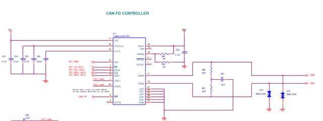
We're designing a custom board with your CAN FD IC [TCAN4550RGYTQ1] and facing GPIO constraints with our main microcontroller. Could you confirm if the following pins are mandatory or optional for proper functioning of the CAN FD IC?
Your prompt response is highly appreciated.
Best regards,
Nitheesh
Hello Nitheesh,
The TCAN4550-Q1 does not require the use of any of these pins for basic CAN FD communication.
The nWKRQ pin is a low-voltage Output pin with similar functionality to the high-voltage Inhibit (INH) pin. This pin is used to indicate that the device is not in Sleep Mode and can be used to control a power regulator or other circuit when transitioning out of Sleep Mode.
The nINT, GPIO1, and GPO2 pins are interrupt pins used to convey real-time information to the MCU. The GPIO1 pin can also be used as a Watchdog Input. But all Interrupt and Status information can be retrieved by polling the SPI registers allowing these pins to be unused. However, this will take extra time through SPI and may reduce the maximum CAN Message Throughput that can be achieved.
The WAKE pin is a High-Voltage Input pin that should not be directly tied to the MCU due to VIH/VIL voltage level incompatibilities. This pin is also optional and only serves to accept a voltage pulse to wake up the device from Sleep Mode such as through a physical switch in the system. There are other methods to wake up the device from Sleep Mode, so this pin is also optional.
Regards,
Jonathan
Hi,
Thanks for your response.
Could you please confirm whether these pins need any specific connections [unused pins] or leave it as a floating pin?
Regards,
Nitheesh
Hi Nitheesh,
The WAKE pin is an input pin that needs to be connected to either GND or VSUP if unused as directed by the datasheet pin description.
All of the other pins are by default output pins and can be left unconnected. The GPIO1 pin can be configured to be an input, but as long as it stays configured as an output it can be left unconnected.
Regards,
Jonathan
Hi,
Thanks for your response.
Additionally we required 24V for Can bus. If i use VBus [4.5V to 5V] as VBat, will it give 24V to CAN bus or anything else to do?
Please check the schematic and advice.
Regards,
Nitheesh
Hi Nitheesh,
The TCAN4550-Q1 can operate with a Vsup supply voltage between 5.5V and 30V. So yes, you can use 24V.
There is an internal LDO that steps the supply voltage down to 5V to power the integrated CAN FD Transceiver. This LDO is capable of supplying additional circuitry through the VCCOUT pin and requires a minimum of 10uF of capacitance on the VCCOUT pin for stability.
Regards,
Jonathan
Hi,
We need to design CAN bus for 24V systems, how much should be the supply voltage i.e. Vsup (pin no.14) of TCAN4550?
Regards,
Nitheesh
Hi Nitheesh,
The Vsup pin has a recommended operating condition range between 5.5V and 30V, so it can be supplied with 24V. The Absolute Maximum Voltage rating for the Vsup pin is 42V which gives some margin for transient spikes between 30V and 42V.
Regards,
Jonathan
Hi,
We have only 5V supply on-board. If we supply the TCAN4550 with 5V, can we connect 24V CAN devices?
Regards,
Nitheesh
No, the minimum Vsup supply voltage for the TCAN4550-Q1 is 5.5V because there is an internal 5V LDO that supplies the CAN transceiver. This internal 5V LDO can't be disabled or bypassed to allow an external 5V supply voltage to be used.
Therefore supplying only 5V to the Vsup supply pin will cause the device to operate in an Under Voltage condition where it will be in a protected mode an prevent normal operation.
Regards,
Jonathan