This thread has been locked.

If you have a related question, please click the "Ask a related question" button in the top right corner. The newly created question will be automatically linked to this question.

TUSB320EVM: Placing the buffer capacitor at power switch

Part Number: TUSB320EVM
Other Parts Discussed in Thread: TUSB320

Hi,

I want to extend my question deriving from https://e2e.ti.com/support/interface-group/interface/f/interface-forum/1298725/tusb320-drd-mode---schematic-proposal?tisearch=e2e-sitesearch&keymatch=tusb320#

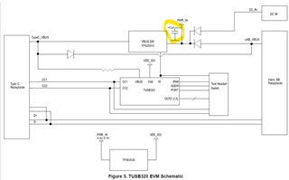
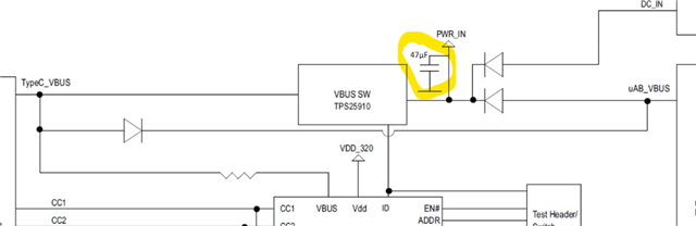
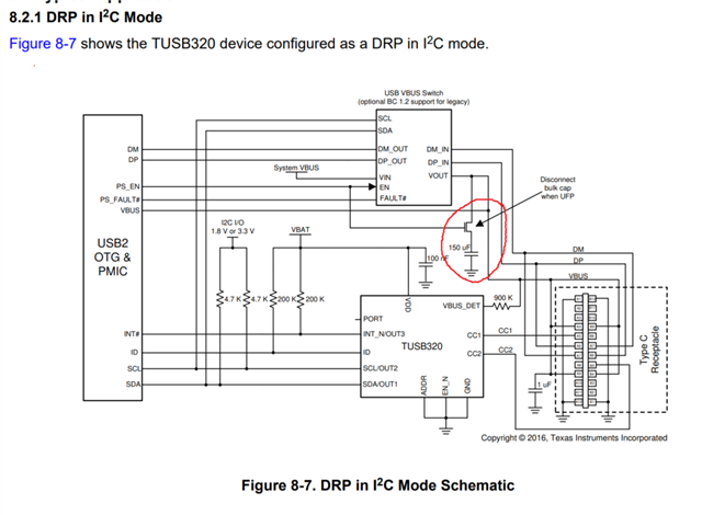
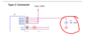
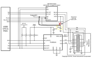
As I have seen at your eval board "TUSB320 Evaluation Module" - you place a buffer capacitor at the IN side of TPS25910RSA.
Can you explain me, why this is placed at the IN side and not at the OUT side of it?

My assumption is, that the capacitor is disconnected immediately in case of micro AB is in UFP mode?
Can you confirm this?

  • Hi Roland,

    That capacitor is what's known as a bypass, or de-coupling capacitor. It reduces AC noise on the power rail coming from the PWR_IN and micAB_VBUS nets.

    I believe there is no capacitor on the OUT side because there is not a particular need to have one. That voltage rail only loops back around to the input, or connects to the VBUS pin on the 320, which is not especially sensitive to small amounts of AC noise.

    You can see similar capacitors used near devices that are more sensitive to AC noise. For example, the VDD_320 net, which powers the TUSB320, and the PWR_IN net near the input to the voltage converter.

    Best,

    Shane

  • Hi Shane,

    I think I have asked the wrong way.
    When I read the USB 2.0 specification it is stated there, that an upfacing port shall have 1-10µF and a downfacing port minimum 120µF.
    So in case of OTG, this must be handled somehow. 
    So I thougth this is realized by placing the capacitor at IN side of the TPS25910RSA?

  • Hi Roland,

    I apologize for misunderstanding and thank you for clarifying. You are correct that our EVM should include capacitors on the VBUS switch output.

    An example of the correct implementation can be seen in the TUSB320 datasheet DRP application.

    This diagram has a 1uF capacitor on VBUS constantly, with another 150uF capacitor that is connected when the 320 is operating as a DFP.

    On the 320 EVM, it seems there is a capacitor for UFP mode on VBUS that is left NC by default. However, I do not see a capacitor to handle DFP mode. 

    So I thougth this is realized by placing the capacitor at IN side of the TPS25910RSA?

    I believe the capacitor at the IN side is for AC noise reduction, and would not realize the spec.

    You're working on a DRP application using the TUSB320 correct? You could use a transistor similar to the diagram from the 320 datasheet.

    Best,

    Shane

  • Hi Shane,

    Thanks for your confirmation.
    Yes, I'm working on a DRP application with TUSB320.

    At OUT side of the power switch I would place a 1µF constantly as you mentioned above (necessary for DFP and UFP mode)..

    To simplify the design, my prefered solution would be to place the 150µF at IN side of the power switch (eg.: TPS25910RSA).
    So I would not need an extra circuit for connecting/disconnecting the 150µF capacitor in DFP mode.

    Do you see any disadvantages/troubles here?

    Best regards,

    Roland

  • Hi Roland,

    The issue I see is that your 150uF capacitance would not be attached directly to the VBUS going out of the connector. The OUT pin and IN pin should be considered as separate nets for the purpose of providing VBUS. You may have AC noise at the output (where the capacitor is expected) that a capacitor on the input cannot compensate for.

    Because of this, you should place the 150uF capacitor on the OUT side of your VBUS switch. This capacitor helps to reduce noise near the VBUS switch when it is providing power.

    Best,

    Shane