Part Number: DP83TC813R-Q1
Hello, Mellin
I continue my questions in email here.
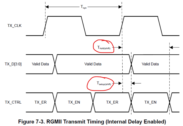
the 100Mbase-T1 RGMII operates in shift mode, communicating with SOC.
in the email, your reply is as below:
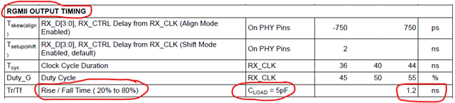
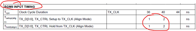
1. about RGMII OUTPUT TIMING:
the RX timing parameters are specified at the ouput pin of RGMII RX interface, right?
the parameters need to match the receiver's(SOC) input specification, right?
2. RGMII TX and RX align mode or delayed(shift) mode configuration
in the snapshot reply above, you have confirmed my understanding OK for the configuration below:
bit 1 =0x0 ==> RX align mode
bit 1 =0x1 ==> RX delay enabled mode
bit 0 =0x0 ==> TX align mode
bit 0 =0x1 ==> TX delay enabled mode
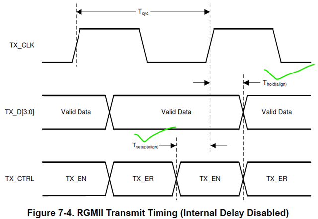
3. about the RGMII TX signals' timing, there are only Tsetup and Thold for align mode, while no Tsetup and Thold for shift mode. please help confirm the range for Tsetup(shift) and Thold(shift).
in the snapshot reply above, the TX shift mode has 0 skew as the same as TX align mode.
(1) could you confirm it? in this way, RGMII TX timing specification on PHY pins are the same for align and shift mode, right?
(2) because the transmitter SOC always has internal delay inside(1.2ns min.), does the delay inside SOC affect the PHY RGMII TX function?
SOC RGMII TX has delay, but PHY RGMII TX needs align timing ==> the interface does not match.
SOC TX delay + PHY TX delay ==> may cause overall TX delay over range for PHY receiving @-40℃ or 95℃ ?? ==> ethernet communication failure @-40℃ or 95℃??
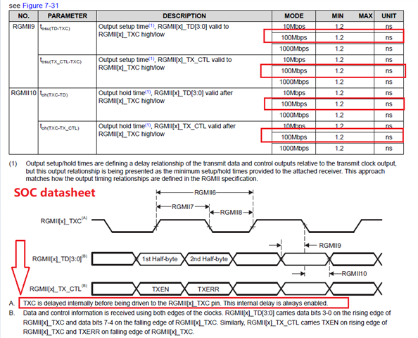
(3) I do not understand the cursor limit for Thold(shift) and Tsetup(shift) in the PHY RGMII TX timing diagram in shift mode. are their cursor limits right? they look strange..
the TX timing diagram in shift mode is easy to understand for me.