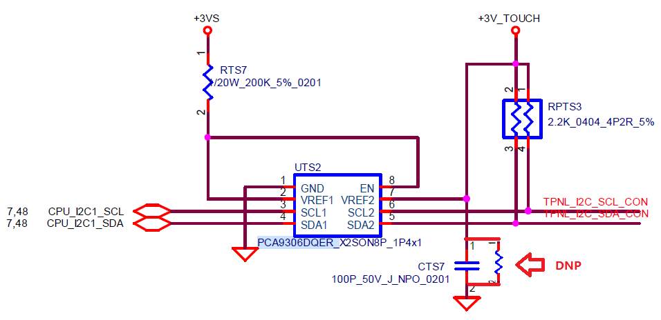
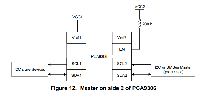
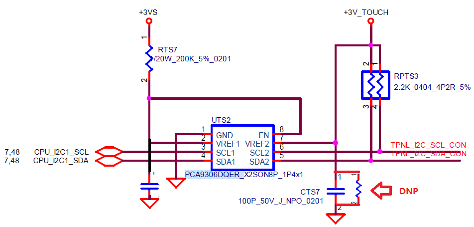
This thread has been locked.
If you have a related question, please click the "Ask a related question" button in the top right corner. The newly created question will be automatically linked to this question.
Hi team,
In the case when both VREF1 and VREF2 is 3.3V defaulted, SCL2/SDA2 is connected to slave with 3.3V pull-high always enabled. To prevent the I2C leakage to master side, customer is considering to connect EN to VREF1 instead of VREF2 ( to shutdown the device when VREF1=0 and VREF2=3.3V). Is there any problem for this application?
Or shall I recommend customer to change SCL1/SDA1 to slave and SCL2/SDA2 to master in order to match with proposed circuit? How shall we connect the pull-up resistors then?
Thanks for your help.
Max
Hey Max,
"customer is considering to connect EN to VREF1 instead of VREF2 ( to shutdown the device when VREF1=0 and VREF2=3.3V). Is there any problem for this application?"
This is okay. They can be interchangeable. I would recommend posting a schematic of their change though so we can triple check to make sure they aren't setting the device up incorrectly.
Thanks,
-Bobby
The enable is set up improperly. The enable pin should be shorted to Vref1 based on your previous statement (not tied directly to 3VS). Currently your set up would allow for very large current from Vref1 to Vref2 if Vref2 is ever GND while Vref1 is powered larger than 0.6V.
PCA9306 will be HI-Z across the SDA/SCL lines if the enable is referenced to GND so there would be no leakage between those nodes. Some leakage could be present if Vref1+EN to Vref2 if Vref2 is zero while Vref1/EN is high.
-Bobby
Hi Bobby,
So in short, changing the pin 8 resistor from 200K to 0 (meaning to short EN/VREF1 both to +3Vs), then no issue for the design?
Thanks
Max
The 200k limiting resistor still needs to be present, the ENABLE pin and the VREF1 pin need to be shorted together then from there a 200k resistor into +3Vs.
I would also place a DNP pull down resistor on Vref2 incase the power supply on Vref2 cannot handle leakage current into that path.
-Bobby
Hi Bobby,
Could you help to confirm if the below design seems OK to you?
And actually in this case, shall we simply change Vref1 to +3V_Touch and Vref2 to +3Vs, where Vref1 will be always 3.3V while Vref2 could be 0/3.3V. And also switch the I2C on both sides. In this case it seems to match the reference better. May I get your confirmation which one is better from design point of view?
Thank you very much.
Max
Hey Max,
Originally, you were saying +3V_Touch was always on while +3Vs could be either on or off.
With how you currently have it set up (meaning Vref1 is tied to EN directly and Vref2 is alone), I would place the power rail which is always on to be on Vref2 and the power rail which could be on or off to Vref1/EN through 200k ohm limiting resistor. That way if the Vref1/EN rail is off, the device would be powered off and HI-Z. If you had it set up opposite where Vref1/EN were always on and Vref2 were sometimes off, you would see some biasing current from Vref1 to Vref2 in the microamp range (which is why I suggested a DNP pull down resistor).
Also, the decoupling cap should be placed on the EN pin as well.
Since you referenced figure 12 from the datasheet, if you want to use that set up instead to line up with the datasheet then you would place the always on power rail on Vref1 instead and the potential on/off rail connect to Vref2/EN through 200k resistor. (EN pin should have a decoupling cap and Vref1 would then have the DNP pull down resistor just in case).
Thanks,
-Bobby