- Ask a related questionWhat is a related question?A related question is a question created from another question. When the related question is created, it will be automatically linked to the original question.
Original question:

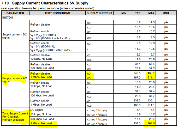
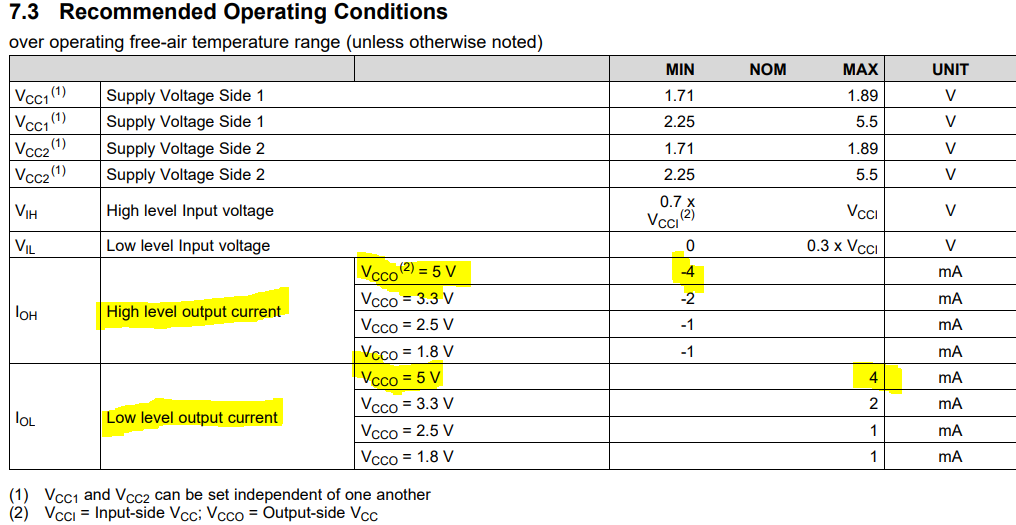
ISO7041: Undetermined output when supply is <1.54V- for how long?
Dear TI Guru,
When VCC1 (Pin1) and VCC2 (Pin16) are un connected in ISO7041, still the currents flow through GND1 (Pin8 ) and GND2(Pin9) though the IO lines at both sides are floating.
The currents are of the order of 2mA & 4mA respectively in the above condition irrespective of EN pins either sides connected to GND or VCC.
And when the VCC1 and VCC2 are given supply of around 5V, the current through pin to pad of pin9 increases by an additional 2mA.
Correct link for the PN = ISO7041 Ultra-Low Power Four-Channel Digital Isolator datasheet (Rev. D) (ti.com)
Thanks in advance for quick help.