


Other Parts Discussed in Thread: CD74HCT4511
Hi Expert,
Customer has question for VDD and A to D pin, If we use P3V3 for VDD and 1.8V voltage level into A~D pin, do we need level shift for 1.8V transfer to 3.3V?
Regards,
Mark
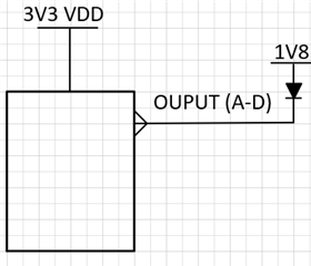
Hi Expert,
Customer has question for VDD and A to D pin, If we use P3V3 for VDD and 1.8V voltage level into A~D pin, do we need level shift for 1.8V transfer to 3.3V?
Regards,
Mark


 If tied to ground when outputs are low they will be 0V