This thread has been locked.
If you have a related question, please click the "Ask a related question" button in the top right corner. The newly created question will be automatically linked to this question.
Tool/software:
Hi,
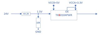
I am using the TXB0104 in my design (schematic attached.
in my design VCCB is 5V and VCCA is 3.3V
- The input to VCCB is off / 24V fed to the pins via resistor split as shown in attached picture.(i,e: 44.2K and 10K to GND)
The issue is that i expected to get 4.42V and i get 1.5V ( I verified and the reason is the connection to the IC).
I tried also to alter the circuit and place on the input pin a p.d of 53.6K to GND and then find resistor so the overall divider will give me >3.25V (Vih min per datasheet)
1. I failed to find any combination to meet my needs.
2. my calculations assumed that maybe there is internal resistance in parallel to the 10K....i got ~4K)....and based on that tried to make divider to get correct Vi...but no success
3. why is it not that straight forward.
4. i also tried to change the device to TXS0104...with external P.U...and no success
Thank you Clemens,
but my issue is not the output. it is the input. instead of having 4.42V i get 1.5V (voltage divider of the 24V input)
Hi Clemens,
I know that each I/O is both input & output.
So how come if my voltage divider supplies <5V it is still trimmed to 1.5V?
Hi Moshe,
It is not recommended to use external pullups/ pulldowns stronger than 50kohms with the TXB/TXS devices due to pullups (TXS) and series resistance (TXB) internally. The effects are documented here in this app note: www.ti.com/.../scea054a.pdf
Regards,
Jack
The voltage is clamped through a diode to VCCB. (When VCCB is off, the current flowing through the diode will raise VCCB.)
For unidirectional signals, you should use a unidirectional translator like the TXU0104.
Dear Clemens,
I think I managed to resolve my issue.
In The datasheet pull up/down it is stated:
"8.3.5 Pullup or Pulldown Resistors on I/O Lines The device is designed to drive capacitive loads of up to 70 pF. The output drivers of the TXB0104 device have low dc drive strength. If pullup or pulldown resistors are connected externally to the data I/Os, their values must be kept higher than 50 kΩ to ensure that they do not contend with the output drivers of the TXB0104 device."
Does it mean only the output driver has this requirement? in the input I can have smaller value P.D? or will it cause malfunction?
BR
ML
The input buffers and output drivers on both sides are always active (when OE is high).
noted.
in my case. where Side B is the input buffer. and A is the driver. is it problematic that the input buffer P.D is less than 50K?
Yes, because the output driver at the same pin might pull the line into the other direction.