This thread has been locked.

If you have a related question, please click the "Ask a related question" button in the top right corner. The newly created question will be automatically linked to this question.

CD74HCT4046A: FSK Modulator - Demodulator Pair using CD74HCT4046A unexpected demodulator functionality

Part Number: CD74HCT4046A
Other Parts Discussed in Thread: CD74HC4046A,

Hello,

I hope you are having a nice day,

We have tried to make a modulator - demodulator pair, like the one shown in document Application Report SLAA618 called "Implementation of FSK Modulation and Demodulation using CD74HC4046A ", but we are using the CD74HCT4046A.
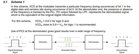
Modulator - Demodulator Pair example


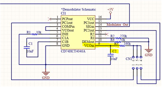
We need to implement a FSK Modulation and Demodulation application, with 2 data "0" and "1", 0 = 1.6 kHz and 1 = 2kHz of frequency respectively with a Bitrate of 400Bits/s, we have consulted the Application Report SLAA618, following this documentation, we try to implement a Modulator and Demodulator, the Modulator works correctly but the demodulator does not, we have changed the values of some components that we think are suitable for our application, as shown in the following image.
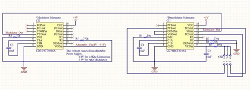
Schematic01


For the Modulator Circuit VCOin Pin we used two voltage values 1.83V for a 1.6kHz signal and 2.3V for a 2kHz signal, “0”=1.83V and “1”=2.3V, for the moment we just input a fixed voltage value to the VCOin pin of the Modulator, either 1.83V or 2.3V.
We hope that if in both demodulator and modulator circuits we use the same resistor and capacitor values on pins R1, C1A and C1B, the output voltage at DEMout of the Demodulator circuit will be the same value of voltage introduced in VCOin of the Modulator Circuit.
For example, if we use a constant 2.3V value in VCOin of the Modulator circuit, the logical thing would be that in the DEMout Pin of the Demodulator circuit we have a signal with a constant voltage of 2.3V, but this is not the case, in the image “IMG001.JPG” we show the behavior we have of the Demodulator Circuit.

IMG001.JPG
In the images "IMG002.JPG" and "IMG003.JPG", the behavior of the DEMout output signal of the demodulator circuit is shown, when a 400hz signal ranging from 1.8V is input into the modulator circuit on the VCOin pin at low level and at high level of 2.3V.

IMG002

IMG003


Do you know why the signal of our Demulator circuit on the DEMout pin has this behavior?


We would like you to help us achieve two things; the first one to improve the signal of the Demodulator Circuit of the DEMout pin, make it equal to the signal that enters the VCOin pin of the Modulator Circuit, the second to know how we can expand the voltage range for the frequencies with which we want to work, currently 1.83V for a 1.6kHZ signal and 2.3V for 2kHZ, gives us a voltage range of .47V, this range or voltage difference is what we would like to make bigger.


I appreciate the time given to this request, have a good day.

Best regards.

Alejandro Ortiz

  • Hi Alejandro,

    I think your issue is with the loop filter. I'd recommend to take a scope shot of the input to the VCO_IN pin of the demodulator.

    The loop filter components shown have a corner frequency of 100 Hz, which is below your data frequency of 400 Hz.  I'd probably try adjusting R3 to 15k and see if that eliminates the issue. If you can watch the input at VCO_IN and adjust R3, you can see how the different loop filter values change the input signal.

  • Hello Emrys,

    Thanks for your help, we have tried your recomendation about R3 value, and now the signal has this following behavior;

    Demodulator SIGin 1K6 Signal and VCOin Scope

    Demodulator 1.6KHZ SIGin and DEMOUT

    Modulator Conditions

    VCOin voltage in = 1.8V Constant (To generate a 1.6khz constant signal

    VCOout = 1.6Khz Signal (Showed in Yellow as "Demodulator SIGin Pin")

    ------------------------------------------------------------------------------------------------------------------------------------------------------------------------------

    Demodulator 2kHZ SIGin and VCOin

    Demodulator 2kHz SIGin and DEMout

    Modulator Conditions

    VCOin voltage in = 1.8V Constant (To generate a 1.6khz constant signal

    VCOout = 2Khz Signal (Showed in Yellow as "Demodulator SIGin Pin")

    ------------------------------------------------------------------------------------------------------------------------------------------------------------------------------

    I would like to know if this IC is correct for the frequencies of our application?

    Could you help me to know how we can increase the voltage range for the Modulator VCOin pin? I mean, now the range starts in 1.8V for 1.6kHz and 2.3V 2kHz, but i would like to separate them for example 1.5V for 1.6kHz and 3.5V for 2KHZ.

    I understand how results a 15K value for R3, but i can't understand why that frequency, i am a little bit confused, could you explain me a little about that?

    Thanks for your help Emrys.

    Best Regards

    Alejandro Ortiz

  • I don't see any problem with using this device for the frequency range you're trying to get, however it may be difficult to get right trying to modulate a 2 kHz signal with a 400 Hz data (800 bps). These two frequencies are pretty close together, so you need good filters to prevent issues -- it looks like reducing R3 did improve things, so you might be able to do this.

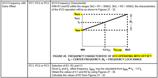
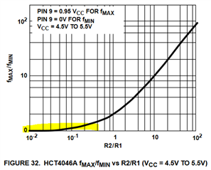
    To change the VCO input voltage range, you need to adjust your timing components. R1, R2, and C1 control the frequency and offset of the device. This image from the datasheet shows the key parameters for using a frequency offset:

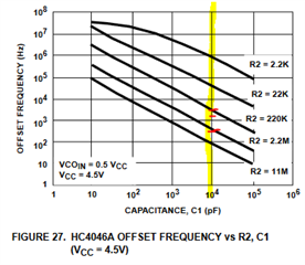
    I did some estimation from the datasheet provided plot to determine R2 should be 1Mohm to get approximately 2kHz offset.  You will likely need to adjust that value to get the exact offset you need (increasing R2 will reduce offset, which will reduce fmin). I'd probably start with about 800k.

    Using this value and your desired min/max frequencies (1.6k and 2.0k), we can get the required ratio of R2 / R1:

    Given that R2 / R1 = 0.6, R1 = R2 / 0.6

    If you're using an 800k resistor for R2, then R1 = 1.33 Mohm.

    Looking at the VCO table, these values are much too large -- the recommended range for R1 and R2 is between 3k and 300k.  You might be able to get this to work, but you might not.

    Which phase comparator (PC1, PC2, or PC3) are you using? It looks like you have all 3 connected so you can try each, but I don't know which is being used for these scope shots.

  • Hi Emrys,
    
    I swear that i had replied to you, but i dont know why mi reply doesnt posted here.

    I tried the values ​​that you recommended and another one with the ratio between R1 and R2 but I did not achieve the results I expected, with the first values ​​my modulator is outside the frequency range of our application. Best regards.
  • We have readed the technical documentation of this chip, but there are things that are very ambiguous and we do not fully understand
    how to calculate the values ​​of the passive components for our application,
    if you could help us with the choice of passive components for our application, it would be great.

    Best Regards
  • Hi Alejandro,

    Emrys mentioned to me that he was going to look into this right now, and he'll get back to you as soon as he can.

    Thanks!

    Chad Crosby

  • Hey Alejandro,

    I put together a spreadsheet in Excel that follows my process for selecting the components. Unfortunately these old PLL's aren't very easy to work with and really require some trial and error to get right for a design.

    If you can increase your C1 value, then you will be able to keep R1 and R2 within the recommended range and I think will have a better chance of meeting your frequency requirements.

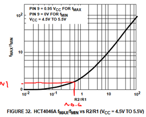
    Note that you are trying to get an f_MAX / f_MIN ratio that is pretty small, so it's not easy to read the values in the datasheet plots:

    The highlighted area include the region of operation for your application, and it's very hard to tell exactly what the correct ratio is. I'd start with 0.2 and decrease the ratio (by increasing R1) until you get to the spot you want to be.

    I've ordered some samples for this device so I can try to duplicate your efforts here - it will be at least a few days before I have them, so you may figure this out before I can test it myself.

    Please see this spreadsheet for my part selection process:

    Excel File