FAQ: TPLD > Current FAQ
TPLD stands for TI Programmable Logic Devices. These devices are a family of programmable logic devices integrating multiple digital and analog functions into a single small package.
Top TI Programmable Logic FAQs
Does TPLD have memory? What kind of memory does TPLD use?
Can a third party program TPLD for me?
Can I permanently program TPLD in-system or in production myself?
What do I use to program TPLD?
Can my TPLD be changed after programming?
Are TPLDs pin-to-pin compatible with competitor devices?
My simulation in ICS is very slow - how do I fix it?
Part Number: TXS0104V
Tool/software:
The biggest difference between the two variants is the ESD protection with TXS-Type offering IEC-ESD protection on the 4-ch/8-ch and higher ESD protection than the TXS-V Type translators. Other spec characteristics are shown below:
|
2-ch |
Spec |
TXS0102 |
TXS0102V |
||
|
ESD |
A-Port |
2.5kV HBM, 1.5kV CDM |
2kV HBM, 500V CDM |
||
|
B-Port |
8kV HBM, 1.5kV CDM |
5kV HBM, 500V CDM |
|||
|
Timing Params. |
Min/ Max |
Typ. only |
|||
|
Q1 Grade Available? |
Y |
Y |
|||
|
|
|||||
|
4-ch |
Spec |
TXS0104E |
TXS0104V |
||
|
ESD |
A-Port |
2kV HBM, 1kV CDM |
2kV HBM, 500V CDM |
||
|
B-Port |
15kV HBM, 8kV IEC-ESD |
5kV HBM, 500V CDM |
|||
|
Timing Params. |
Min/ Max |
Typ. only |
|||
|
Q1 Grade Available? |
Y |
Y |
|||
Part Number: SN74HCS08
Tool/software:
App Note: Optimizing Board Design for Supply Constrained Environments
Dual foot-printing packages is the practice of overlaying a package's layout on top of another package. This allows more flexibility in system designs when supply issues are a main constraint.
The following are some combinations of packages that are recommend from our team. If there is a combination not listed, this does not mean it cannot be dual foot-printed. In general, there is nothing stopping any two packages from being foot-printed together. However, clearance rules will still need to be observed. There will be at least 5 mil clearance between any traces.
PW (14/16) -> DYY (14/16)


PW (20) -> DGS
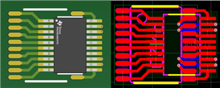
PW (14/16) -> BQB (14) / BQA (16)
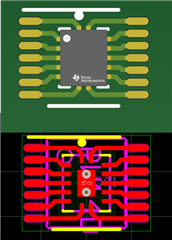

NS (16) -> BQB
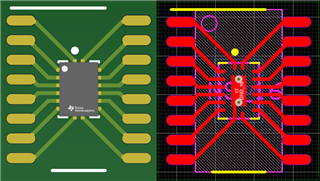
NS (20) -> RKS
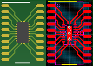
DBV -> DCK

DCT -> DCU
FAQ: Logic and Voltage Translation > Auto-Bidirectional Level-Shifters > Current FAQ
In most cases, it is recommended to test with the device EVM instead as it yields much more accurate results under specific system loading. Simulation results captured in IBIS should not be relied entirely on signal integrity expectations due to the drive strength limitations of the LSF/TXB/TXS devices. The links below are given depending on the auto-bidirectional families EVMs.
Below are recommendations on how the models should be configured/ selected depending on translator used:
For signal integrity simulations with LSF device, models ending with “s” may be used to provide switch behavior during translation. IO models not denoted by “s” are known as termination models providing just ground clamp characteristics i.e during a HIGH-Z state.
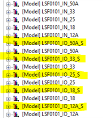
Since the LSF-type translators is comprised of passive FETs, the IO model should be selected depending on the voltage that output signal is being translated to. For example, if 1.8V to 3.3V simulation is desired, LSF0101_IO_33_S should be used to observe 3.3V output behavior. If the output side voltage is 1.8V, the LSF0101_IO_18_S model may be used to observe 1.8V output behavior.
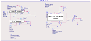
For signal integrity simulation with the TXB device, OS models and the series models should be used in conjunction to portray output behavior more accurately. The OS model describes the behavior of the one-shot impedance, while the IO model replicates the internal series resistors impedance. See below example simulation:
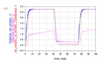
By combining both the series resistance model and the one-shot model of the device (red waveform), a more accurate representation of the output behavior can be shown compared to the output waveform of the individual OS model and IO model.
FAQ: Logic and Voltage Translation > Fixed DIR / DIR CNTRL Level-Shifters >> Current FAQ
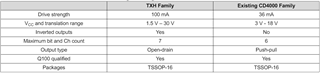
Existing level-shifters typically support up to 18 V. For up to 30 V, see the TXH0137D family highlighted below.
For more information, see Leveraging TXH for High Voltage Level Shifting
FAQ: Logic and Voltage Translation > Fixed DIR / DIR CNTRL Level-Shifters >> Current FAQ
Consider the worst-case values in the electrical characteristics table; VT+(max) and VT−(min) are what matters for VIH and VIL respectively. See Understanding Schmitt Trigger.
However, the VOL / VOH values into the level-shifter are most likely different than your actual worst case. They are specified for a certain output current and the actual output current will be much smaller when connected to a high-impedance CMOS input. Hence, the actual output voltages into the level-shifter will be near GND or VCC.
Note, CMOS outputs can be modeled as resistors; see [FAQ] What is the output voltage (VOH or VOL) when the output current is X or the supply voltage is Y?)
FAQ: Logic and Voltage Translation > Auto-Bidirectional Level-Shifters > Fixed DIR / DIR CNTRL Level-Shifters >> Current FAQ
Choosing a high drive strength device depends on the below:
For more information, see Understanding Transient Drive Strength vs. DC Drive Strength in CMOS Output Buffers
FAQ: Logic and Voltage Translation > Auto-Bidirectional Level-Shifters >> Current FAQ
The most common reason is due to impedance mismatches.
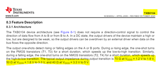
TXB0304 specifies a stronger output impedance than TXB0104, as highlighted below:
This implies TXB0104's output impedance is matched closer to the typical 50 ohms transmission line.
When using TXB0304, appropriate impedance matching is recommended.
See [FAQ] Can I estimate appropriate dampening resistor value for level-shifter outputs?
FAQ: Logic and Voltage Translation > Auto-Bidirectional Level-Shifters >> Current FAQ
To mitigate oscillation concerns with devices with edge rate accelerators / one-shots such as TXB / TXS devices, consider below:
For more information see Do’s and Don’ts for TXB and TXS Voltage Level-Shifters with Edge Rate Accelerators.
