This thread has been locked.

If you have a related question, please click the "Ask a related question" button in the top right corner. The newly created question will be automatically linked to this question.

EK-TM4C1294XL: EK-TM4C1294XL

Part Number: EK-TM4C1294XL

Hi,

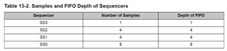
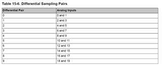
I want to read 3 analog voltage signals in an experiment. I want to implement this with the EK-TM4C1294XL part without any additional hardware. From what I have read in the datasheet, it seems so, because it consists of 2 ADC modules to which 20 analog inputs can be connected. I understand that the reading of the 3 then could be done on a single ADC, sequentially. In case you can really do that, what is the maximum sampling frequency at which I can read the 3 signals ?

Thanks in advance for your help
Regards
Adrian Llanos

  • Hi,

      Yes, you can certainly use one ADC to read 3 analog inputs. Each ADC module has four Sample Sequencers. Different sample sequencers can support different number of samples. Refer to the datasheet for details. See below. As you can see you can use either SS0, SS1 or SS2 to sample three inputs.  

    Below example code would use SS0 to sample three inputs (AIN0, AIN1, AIN2) triggered by the processor. By default, the ADC module uses PIOSC (16Mhz) as the source clock for ADCCLK. This will give you a 1MSPS. 

        ADCSequenceConfigure(ADC0_BASE, 0, ADC_TRIGGER_PROCESSOR, 0);
    
        ADCSequenceStepConfigure(ADC0_BASE, 0, 0, ADC_CTL_CH0 );
    
        ADCSequenceStepConfigure(ADC0_BASE, 0, 1, ADC_CTL_CH1 );
    
        ADCSequenceStepConfigure(ADC0_BASE, 0, 2, ADC_CTL_CH2 | ADC_CTL_IE |
                                 ADC_CTL_END);
    
        ADCSequenceEnable(ADC0_BASE, 0);

  • Thank you Charles, i see.  One thing i wanted to ask you too is about the possibility of reading single or differential signals. I understand that the range of the ADCs is 0 to VDDA for single type analog inputs and -VDDA to VDDA for differential type analog inputs. From what I have read in the documentation, VDDA is 3.3 V (table 27-44), so could three analog signals ranging from -2 to 2 volts be read (in differential mode) in one of the three modes you have told me about (SS0,SS1 or SS2) right ? 

  • If you use differential mode then you can only use SS0 to sample 3 pairs of differential inputs. Three pairs will take up 6 inputs for which only SS0 can support, not SS1 and SS2 which can only take 4 inputs unless you limit to two differential pairs. Refer to the datasheet for details. 

    When a sequence step is configured for differential sampling, the input pair to sample must be
    configured in the ADCSSMUXn register. Differential pair 0 samples analog inputs 0 and 1; differential pair 1 samples analog inputs 2 and 3;

    so could three analog signals ranging from -2 to 2 volts be read

    Please refer to the datasheet. 

    ■ Input Positive Voltage: VIN+ = VIN_EVEN (even channel)
    ■ Input Negative Voltage: VIN- = VIN_ODD (odd channel)
    The input differential voltage is defined as: VIND = VIN+ - VIN-, therefore:
    ■ If VIND = 0, then the conversion result = 0x800
    ■ If VIND > 0, then the conversion result > 0x800 (range is 0x800–0xFFF)
    ■ If VIND < 0, then the conversion result < 0x800 (range is 0–0x800)
    When using differential sampling, the following definitions are relevant:
    ■ Input Common Mode Voltage: VINCM = (VIN+ + VIN-) / 2
    ■ Reference Positive Voltage: VREFP
    ■ Reference Negative Voltage: VREFN
    ■ Reference Differential Voltage: VREFD = VREFP - VREFN
    ■ Reference Common Mode Voltage: VREFCM = (VREFP + VREFN) / 2
    The following conditions provide optimal results in differential mode:
    ■ Both VIN_EVEN and VIN_ODD must be in the range of (VREFP to VREFN) for a valid conversion
    result
    The maximum possible differential input swing, or the maximum differential range, is: -VREFDto
    +VREFD, so the maximum peak-to-peak input differential signal is (+VREFD - -VREFD) = 2 *
    VREFD= 2 * (VREFP - VREFN)

  • I see. I think i understand it. What I am trying to do is something similar to what was asked in this thread. 

    https://e2e.ti.com/support/microcontrollers/arm-based-microcontrollers-group/arm-based-microcontrollers/f/arm-based-microcontrollers-forum/787231/tm4c123gh6pm-adc-using-differential-mode-is-noisy

    My idea was like this:

    I understand that this cannot be done because the ADC pins are not designed to read unipolar signals (as it says in the datasheet, "Both VIN_EVEN and VIN_ODD must be in the range of (VREFP to VREFN) for a valid conversion result"). Therefore, the only possible solution is to condition the signal to go from the range -2 to 2 v to 0 to 3.3 v, right ?

  • Therefore, the only possible solution is to condition the signal to go from the range -2 to 2 v to 0 to 3.3 v, right ?

    That is correct.