This thread has been locked.

If you have a related question, please click the "Ask a related question" button in the top right corner. The newly created question will be automatically linked to this question.

MCU-PLUS-SDK-AM263X: MCU-PLUS-SDK-AM263X

Part Number: MCU-PLUS-SDK-AM263X
Other Parts Discussed in Thread: SYSCONFIG

Tool/software:

MCU-PLUS-SDK-AM263X: Continuous sampling of multiple ADCs to DMA buffers

I want to configure multiple ADC channels to continuously read voltage and store the samples to RAM using DMA.

Referring to SDK example: adc_soc_continuous_dma

I have this example working, but the SDK example fills the DMA buffers, and then stops. 

I want to modify example such that ADC conversion is continuous for defined number of samples.

I experimented removing the function calls in the ISRs (seen here) which I suspected may be stopping the 'continuous ADC to DMA' that I want. 

  • Hello Yogesh,

    Can you include the ISR code that you modified?

    Best Regards,

    Zackary Fleenor

  • 8814.adc_soc_continuous_dma.c
    /*
     *  Copyright (C) 2023 Texas Instruments Incorporated
     *
     *  Redistribution and use in source and binary forms, with or without
     *  modification, are permitted provided that the following conditions
     *  are met:
     *
     *    Redistributions of source code must retain the above copyright
     *    notice, this list of conditions and the following disclaimer.
     *
     *    Redistributions in binary form must reproduce the above copyright
     *    notice, this list of conditions and the following disclaimer in the
     *    documentation and/or other materials provided with the
     *    distribution.
     *
     *    Neither the name of Texas Instruments Incorporated nor the names of
     *    its contributors may be used to endorse or promote products derived
     *    from this software without specific prior written permission.
     *
     *  THIS SOFTWARE IS PROVIDED BY THE COPYRIGHT HOLDERS AND CONTRIBUTORS
     *  "AS IS" AND ANY EXPRESS OR IMPLIED WARRANTIES, INCLUDING, BUT NOT
     *  LIMITED TO, THE IMPLIED WARRANTIES OF MERCHANTABILITY AND FITNESS FOR
     *  A PARTICULAR PURPOSE ARE DISCLAIMED. IN NO EVENT SHALL THE COPYRIGHT
     *  OWNER OR CONTRIBUTORS BE LIABLE FOR ANY DIRECT, INDIRECT, INCIDENTAL,
     *  SPECIAL, EXEMPLARY, OR CONSEQUENTIAL DAMAGES (INCLUDING, BUT NOT
     *  LIMITED TO, PROCUREMENT OF SUBSTITUTE GOODS OR SERVICES; LOSS OF USE,
     *  DATA, OR PROFITS; OR BUSINESS INTERRUPTION) HOWEVER CAUSED AND ON ANY
     *  THEORY OF LIABILITY, WHETHER IN CONTRACT, STRICT LIABILITY, OR TORT
     *  (INCLUDING NEGLIGENCE OR OTHERWISE) ARISING IN ANY WAY OUT OF THE USE
     *  OF THIS SOFTWARE, EVEN IF ADVISED OF THE POSSIBILITY OF SUCH DAMAGE.
     */
    
    #include <kernel/dpl/DebugP.h>
    #include <kernel/dpl/ClockP.h>
    #include <kernel/dpl/SemaphoreP.h>
    #include <kernel/dpl/HwiP.h>
    #include <drivers/epwm.h>
    #include <drivers/adc.h>
    #include "ti_drivers_config.h"
    #include "ti_drivers_open_close.h"
    #include "ti_board_open_close.h"
    
    /*
     * This example sets up two ADC channels to convert simultaneously. The
     * results will be transferred by DMA into a buffer in RAM.
     *
     * errata i2355 for AM263x:
     *  DMA trigger from the ADC INT (Late) occurs just before the Result space updation,
     *  as a result of which the stale data from the result space will be transferred by
     *  DMA.
     *  Workaround:
     *      use an empty channel transfer before the Actual transfer.
     *
     * It configures ePWM0 to trigger SOC0 on ADC1 and ADC2. EPWM is only used to
     * trigger the first ADC conversion. INT0 of ADC1 is configured to generate
     * interrupt after first conversion and will then disable EPWM SOC generation.
     * INT1 of both ADC's is configured to enable continuous conversion.
     *
     * DMA channel 0 is triggered at EOC0 of ADC1 and will copy conversion result
     * to a empty buffer in RAM, and triggers DMA Channel 1 to copy actual conversion
     * result to result buffer in RAM. Similarly, DMA Channel 2 is triggered at ADC 2 EOC0
     * and transfers ADC 2 result space an empty buffer in RAM and .
     * DMA will generate interrupt after the buffer is filled and will stop conversion on both ADCs.
     *
     * The below watch variables can be used to view ADC conversion results.
     *
     * External Connections
     * ADC1_AIN0 and ADC2_AIN0 pins should be connected to signals to be converted.
     * AM263X-CC E2:
     *  - Feed the External Volatage to the following
     *      - ADC1_AIN0 :   HSEC-PIN 12
     *      - ADC2_AIN0 :   HSEC-PIN 31
     * AM263X-LP :
     *  - Feed the External Volatage to the following
     *      - ADC1_AIN0 :   J1/3 24
     *      - ADC2_AIN0 :   J1/3 25
     *
     * Watch Variables
     * gAdc1DataBuffer - Buffers which stores conversion results from ADC1
     * gADC2DataBuffer - Buffers which stores conversion results from ADC2
     */
    
    /* Size of buffer for storing conversion results */
    #define RESULTS_BUFFER_SIZE     1024*16
    /* Event queue to be used for EDMA transfer */
    #define EDMA_TEST_EVT_QUEUE_NO_0  0U
    #define EDMA_TEST_EVT_QUEUE_NO_1  1U
    
    /* DMA channel number to transfer ADC1 and ADC2 conversion results*/
    /* the following channels will be used for empty transaction to comply to errata i2355
       these chain the ADC result data transfer */
    #define ADC1_EDMA_CHANNEL       (DMA_TRIG_XBAR_EDMA_MODULE_0)
    #define ADC2_EDMA_CHANNEL       (DMA_TRIG_XBAR_EDMA_MODULE_2)
    /* Note: the actual transfer channels are configured for EDMA_RESOURCE_ALLOC_ANY,
    typically selecting the next available channels
        in this case, DMA_TRIG_XBAR_EDMA_MODULE_1 and DMA_TRIG_XBAR_EDMA_MODULE_3 hold the actual transfer.*/
    
    /* Global variables and objects */
    /* Buffers to store conversion results from ADC1 and ADC2 */
    uint16_t gAdc1DataBuffer[RESULTS_BUFFER_SIZE];
    uint16_t gAdc2DataBuffer[RESULTS_BUFFER_SIZE];
    uint16_t gUnusedBuffer[RESULTS_BUFFER_SIZE];
    
    static HwiP_Object  gAdcHwiObject;
    /* Semaphore to indicate transfer completion */
    static SemaphoreP_Object gEdmaTransferDoneSem;
    /* ADC instance base addresses */
    uint32_t gAdc1baseAddr = CONFIG_ADC1_BASE_ADDR;
    uint32_t gAdc2baseAddr = CONFIG_ADC2_BASE_ADDR;
    
    /* Function Prototypes */
    uint16_t App_dmaConfigure(const uint16_t *table, uint16_t table_size,
            EDMA_Handle dma_handle, uint32_t dma_ch,
            uint32_t adc_base, uint32_t *tccAlloc, uint32_t event_queue_number);
    static void App_adcISR(void *args);
    static void App_dmach0ISR(Edma_IntrHandle intrHandle, void *args);
    
    void adc_soc_continuous_dma_main(void *args)
    {
        int32_t  status;
        Edma_IntrObject     intrObj;
        HwiP_Params  hwiPrms;
        uint32_t     loopCnt = 0;
        uint32_t tccAlloc0, tccAlloc1;
    
        /* Open drivers to open the UART driver for console */
        Drivers_open();
        Board_driversOpen();
    
        DebugP_log("ADC Continuous DMA transfer Test Started ...\r\n");
    
        /* Initialize both the result buffers with zeroes */
        for(loopCnt = 0U; loopCnt < RESULTS_BUFFER_SIZE; loopCnt++)
        {
            gUnusedBuffer[loopCnt] = 0U;
            gAdc1DataBuffer[loopCnt] = 0U;
            gAdc2DataBuffer[loopCnt] = 0U;
        }
    
        /* Perform a cache write back to the result buffers */
        CacheP_wb((void *)gAdc1DataBuffer, RESULTS_BUFFER_SIZE*2, CacheP_TYPE_ALL);
        CacheP_wb((void *)gAdc2DataBuffer, RESULTS_BUFFER_SIZE*2, CacheP_TYPE_ALL);
    
        /* Register & enable interrupt */
        HwiP_Params_init(&hwiPrms);
        hwiPrms.intNum      = CSLR_R5FSS0_CORE0_CONTROLSS_INTRXBAR0_OUT_0;
        hwiPrms.callback    = &App_adcISR;
        status              = HwiP_construct(&gAdcHwiObject, &hwiPrms);
        DebugP_assert(status == SystemP_SUCCESS);
    
        /* Create a semaphore to signal EDMA transfer completion */
        status = SemaphoreP_constructBinary(&gEdmaTransferDoneSem, 0);
        DebugP_assert(SystemP_SUCCESS == status);
    
        /* Configure DMA channels to transfer both ADC results */
        App_dmaConfigure(gAdc1DataBuffer, RESULTS_BUFFER_SIZE, gEdmaHandle[0],
                    ADC1_EDMA_CHANNEL, CONFIG_ADC1_RESULT_BASE_ADDR, &tccAlloc0, EDMA_TEST_EVT_QUEUE_NO_0);
    
        App_dmaConfigure(gAdc2DataBuffer, RESULTS_BUFFER_SIZE, gEdmaHandle[0],
                    ADC2_EDMA_CHANNEL, CONFIG_ADC2_RESULT_BASE_ADDR, &tccAlloc1, EDMA_TEST_EVT_QUEUE_NO_1);
    
        /* Register interrupt */
        intrObj.tccNum = tccAlloc0;
        intrObj.cbFxn  = &App_dmach0ISR;
        intrObj.appData = (void *) &gEdmaTransferDoneSem;
        status = EDMA_registerIntr(gEdmaHandle[0], &intrObj);
        DebugP_assert(status == SystemP_SUCCESS);
    
        /* Clear ADC Interrupt status */
        ADC_clearInterruptStatus(gAdc1baseAddr,ADC_INT_NUMBER1);
        ADC_clearInterruptStatus(gAdc1baseAddr,ADC_INT_NUMBER2);
        ADC_clearInterruptStatus(gAdc2baseAddr,ADC_INT_NUMBER1);
        ADC_clearInterruptStatus(gAdc2baseAddr,ADC_INT_NUMBER2);
    
        /* Enable event counter init for SOCA */
        EPWM_enableADCTriggerEventCountInit(CONFIG_EPWM0_BASE_ADDR, EPWM_SOC_A);
        /* Set the event counter init value to 0 */
        EPWM_setADCTriggerEventCountInitValue(CONFIG_EPWM0_BASE_ADDR, EPWM_SOC_A, 0);
        /* Force the event counter init value to event counter */
        EPWM_forceADCTriggerEventCountInit(CONFIG_EPWM0_BASE_ADDR, EPWM_SOC_A);
        EPWM_clearADCTriggerFlag(CONFIG_EPWM0_BASE_ADDR, EPWM_SOC_A);
    
        /* Enable ADC Trigger from EPWM to start ADC conversion */
    	EPWM_enableADCTrigger(CONFIG_EPWM0_BASE_ADDR, EPWM_SOC_A);
    	EPWM_setADCTriggerSource(CONFIG_EPWM0_BASE_ADDR, EPWM_SOC_A, EPWM_SOC_TBCTR_ZERO, EPWM_SOC_TBCTR_ZERO);
    	EPWM_setADCTriggerEventPrescale(CONFIG_EPWM0_BASE_ADDR, EPWM_SOC_A, 1);
    	EPWM_setTimeBaseCounterMode(CONFIG_EPWM0_BASE_ADDR, EPWM_COUNTER_MODE_UP);
    
        /*
         * Wait while DMA transfers ADC conversion results to buffer.
        */
        SemaphoreP_pend(&gEdmaTransferDoneSem, SystemP_WAIT_FOREVER);
    
        /* Invalidate destination buffer */
        CacheP_inv((void *)gUnusedBuffer, RESULTS_BUFFER_SIZE*2, CacheP_TYPE_ALL);
        CacheP_inv((void *)gAdc1DataBuffer, RESULTS_BUFFER_SIZE*2, CacheP_TYPE_ALL);
        CacheP_inv((void *)gAdc2DataBuffer, RESULTS_BUFFER_SIZE*2, CacheP_TYPE_ALL);
    
        DebugP_log("ADC1 : ADC2 Result register value -\r\n");
    
        loopCnt = 0;
        /* Print few elements from the result buffer */
        while(loopCnt < RESULTS_BUFFER_SIZE)
        {
            DebugP_log("%d : %d\r\n", gAdc1DataBuffer[loopCnt], gAdc2DataBuffer[loopCnt]);
            loopCnt += 100;
        }
    
        DebugP_log("ADC Continuous DMA transfer Test Passed\r\n");
        DebugP_log("All tests have passed!!\r\n");
    
        Board_driversClose();
        Drivers_close();
    }
    
    uint16_t App_dmaConfigure(
            const uint16_t *table, uint16_t table_size,
            EDMA_Handle dma_handle, uint32_t dma_ch,
            uint32_t adc_base, uint32_t *tccAlloc, uint32_t event_queue_number)
    {
    
        uint32_t            baseAddr, regionId;
        EDMACCPaRAMEntry    empty_edmaParam, edmaParam;
        uint32_t            empty_dmaCh, dmaCh, empty_tcc, tcc, empty_param, param;
        // EDMACCPaRAMEntry    empty_edmaParam;
        // uint32_t            empty_dmaCh, empty_tcc, empty_param;
        int32_t             testStatus = SystemP_SUCCESS;
    
        /* Enable only TC and ITC chaining on dmaCh0.
           TC and ITC interrupt enable not required. */
        uint32_t chainOptions = (EDMA_OPT_TCCHEN_MASK |
                                 EDMA_OPT_ITCCHEN_MASK);
    
        baseAddr = EDMA_getBaseAddr(gEdmaHandle[0]);
        DebugP_assert(baseAddr != 0);
    
        regionId = EDMA_getRegionId(gEdmaHandle[0]);
        DebugP_assert(regionId < SOC_EDMA_NUM_REGIONS);
    
        empty_dmaCh = dma_ch;
        testStatus = EDMA_allocDmaChannel(gEdmaHandle[0], &empty_dmaCh);
        DebugP_assert(testStatus == SystemP_SUCCESS);
    
        /* typically allocates the next available channel */
        empty_tcc = EDMA_RESOURCE_ALLOC_ANY;
        testStatus = EDMA_allocTcc(gEdmaHandle[0], &empty_tcc);
        DebugP_assert(testStatus == SystemP_SUCCESS);
    
        empty_param = EDMA_RESOURCE_ALLOC_ANY;
        testStatus = EDMA_allocParam(gEdmaHandle[0], &empty_param);
        DebugP_assert(testStatus == SystemP_SUCCESS);
    
        dmaCh = EDMA_RESOURCE_ALLOC_ANY;
        testStatus = EDMA_allocDmaChannel(gEdmaHandle[0], &dmaCh);
        DebugP_assert(testStatus == SystemP_SUCCESS);
    
        tcc = EDMA_RESOURCE_ALLOC_ANY;
        testStatus = EDMA_allocTcc(gEdmaHandle[0], &tcc);
        DebugP_assert(testStatus == SystemP_SUCCESS);
        /* Passing back the Channel parameter to register the interrupt ISR*/
        *tccAlloc = tcc;
    
        param = EDMA_RESOURCE_ALLOC_ANY;
        testStatus = EDMA_allocParam(gEdmaHandle[0], &param);
        DebugP_assert(testStatus == SystemP_SUCCESS);
    
        /* Request channel */
        EDMA_configureChannelRegion(baseAddr, regionId, EDMA_CHANNEL_TYPE_DMA,
             empty_dmaCh, empty_tcc, empty_param, event_queue_number);
    
        /* Program Param Set */
        EDMA_ccPaRAMEntry_init(&empty_edmaParam);
        empty_edmaParam.srcAddr       = (uint32_t) SOC_virtToPhy((void *)(adc_base+CSL_ADC_RESULT_ADCRESULT0));
        empty_edmaParam.destAddr      = (uint32_t) SOC_virtToPhy((void *)gUnusedBuffer);
        empty_edmaParam.aCnt          = (uint16_t) 2;
        empty_edmaParam.bCnt          = (uint16_t) table_size;
        empty_edmaParam.cCnt          = (uint16_t) 1;
        empty_edmaParam.bCntReload    = 0;
        empty_edmaParam.srcBIdx       = (int16_t) EDMA_PARAM_BIDX(0);
        empty_edmaParam.destBIdx      = (int16_t) EDMA_PARAM_BIDX(2);
        empty_edmaParam.srcCIdx       = (int16_t) 0;
        empty_edmaParam.destCIdx      = (int16_t) 0;
        empty_edmaParam.linkAddr      = 0xFFFFU;
        empty_edmaParam.srcBIdxExt    = (int8_t) EDMA_PARAM_BIDX_EXT(0);
        empty_edmaParam.destBIdxExt   = (int8_t) EDMA_PARAM_BIDX_EXT(2);
        empty_edmaParam.opt           = (EDMA_OPT_TCINTEN_MASK | EDMA_OPT_ITCINTEN_MASK |
                                  ((((uint32_t)empty_tcc) << EDMA_OPT_TCC_SHIFT) & EDMA_OPT_TCC_MASK));
        /* Enabling in options for the,
            the Transfer-complete Interrupt          --> After total data is transferred
        ,   Intermediate transfer complete interrupt --> After each A data chunk transfer is comeplete
                this will be used for the chaining of the actual transfer.
        */
    
        EDMA_setPaRAM(baseAddr, empty_param, &empty_edmaParam);
    
        EDMA_configureChannelRegion(baseAddr, regionId, EDMA_CHANNEL_TYPE_DMA,
                dmaCh, tcc, param, event_queue_number);
    
        /* Program Param Set */
        EDMA_ccPaRAMEntry_init(&edmaParam);
        edmaParam.srcAddr       = (uint32_t) SOC_virtToPhy((void *)(adc_base+CSL_ADC_RESULT_ADCRESULT0));
        edmaParam.destAddr      = (uint32_t) SOC_virtToPhy((void *)table);
        edmaParam.aCnt          = (uint16_t) 2;
        edmaParam.bCnt          = (uint16_t) table_size;
        edmaParam.cCnt          = (uint16_t) 1;
        edmaParam.bCntReload    = 0;
        edmaParam.srcBIdx       = (int16_t) EDMA_PARAM_BIDX(0);
        edmaParam.destBIdx      = (int16_t) EDMA_PARAM_BIDX(2);
        edmaParam.srcCIdx       = (int16_t) 0;
        edmaParam.destCIdx      = (int16_t) 0;
        edmaParam.linkAddr      = 0xFFFFU;
        edmaParam.srcBIdxExt    = (int8_t) EDMA_PARAM_BIDX_EXT(0);
        edmaParam.destBIdxExt   = (int8_t) EDMA_PARAM_BIDX_EXT(2);
        edmaParam.opt           = (EDMA_OPT_TCINTEN_MASK |
                                  ((((uint32_t)tcc) << EDMA_OPT_TCC_SHIFT) & EDMA_OPT_TCC_MASK));
        /* Enabling the Interrupt for Transfer complete of all the data */
        EDMA_setPaRAM(baseAddr, param, &edmaParam);
    
        /* Chain the empty transfer to the actual transfer.
        Chain options include Total transfer completion and intermediate channel completion flags
        from empty channel*/
    
        EDMA_chainChannel(baseAddr, empty_param, dmaCh, chainOptions);
    
        /* Enabling the transfer region for empty channel for the trigger mode set in the Syscfg through
        the DMA Xbars adn DMA TRIG Xbars.*/
        EDMA_enableTransferRegion(baseAddr, regionId, empty_dmaCh,
                                  EDMA_TRIG_MODE_EVENT);
        return testStatus;
    }
    
    void App_adcISR(void *args)
    {
        /* Remove ePWM trigger */
        EPWM_disableADCTrigger(CONFIG_EPWM0_BASE_ADDR, EPWM_SOC_A);
    
        /* Disable this interrupt from happening again */
        ADC_disableInterrupt(gAdc1baseAddr, ADC_INT_NUMBER1);
    }
    
    void App_dmach0ISR(Edma_IntrHandle intrHandle, void *args)
    {
        SemaphoreP_Object *semObjPtr = (SemaphoreP_Object *)args;
        DebugP_assert(semObjPtr != NULL);
    
        /* Stop the ADCs by removing the trigger for SOC0 */
        ADC_setInterruptSOCTrigger(gAdc1baseAddr, ADC_SOC_NUMBER0,
                                   ADC_INT_SOC_TRIGGER_NONE);
        ADC_setInterruptSOCTrigger(gAdc2baseAddr, ADC_SOC_NUMBER0,
                                   ADC_INT_SOC_TRIGGER_NONE);
    
        /* Post the semaphore to signal end of DMA transfer */
        SemaphoreP_post(semObjPtr);
    }

    I am using attached code from TI SDK (adc_soc_continuous_dma.c). I have just commented out ADC Stopping from App_dmach0ISR(). Our requirement is to continuously sample 256 ADC using DMA and repeat that process again for ever.

    There is one thread from TollMan where similar issue was resolved. Final working code is not posted, so could not understand the solution.

  • waiting for the response and solution.

  • Hello Yogesh,

    Apologies for the delay as our expert was out of office. Please provide 1-2 more days for review and additional feedback.

    Best Regards,

    Zackary Fleenor

  • Hey Yogesh,

    Can you include the link for the previous E2E post you mentioned?

    Best Regards,

    Zackary Fleenor

  • Fleenor - Here is the link:

    MCU-PLUS-SDK-AM263X: Continuous sampling of multiple ADCs to DMA buffers - Arm-based microcontrollers forum - Arm-based microcontrollers - TI E2E support forums

    I was referring to. I am facing the exact same issue and want to the solution that TollMan implemented as suggested by Madhav and I need help to understand the solution. Please help on priority.

  • Fleenor - This is very unfortunate that I am not getting reply. I am stuck with this issue and no support from TI is bad.

    Essentially here is what I am trying to finally achieve - Sample ADC0 to ADC5 all 6 channels at a frequency of 1ms.

    To start with I have taken the "adc_soc_continuous_dma" code from TI examples.

    Modified the example code to sample ADC0-AIN0, ADC1-AIN0 and ADC2-AIN0 continuously.

    I could successfully modify the code to do a continuous DMA Link transfer for ADC0-AIN0 and ADC1-AIN1

    BUT ADC2-AIN0 data is NOT being read successfully. 

    I am attaching the code from your review. Please help.adc_soc_continuous_dma_am263x-lp_r5fss0-0_nortos_ti-arm-clang.zip

  • Hi Yogesh

    Apologies for the delay. I am working on your issue as of now, please give me some time to bring the implementation to you.

    Regards,
    Akshit

  • Hi Akshit - I have attached the zip of my project based on the "adc_soc_continuous_dma" example code. Please have a look.

    Below are the ADC reading log.

    ADC0 : ADC1 : ADC2 : ADC3 : ADC4
    79 : 74: 0
    81 : 79: 0
    83 : 82: 0
    86 : 85: 0
    88 : 86: 0
    90 : 87: 0
    89 : 86: 0
    86 : 85: 0
    84 : 82: 0
    80 : 76: 0

    ADC0 : ADC1 : ADC2 : ADC3 : ADC4
    78 : 76: 0
    77 : 76: 0
    77 : 76: 0
    77 : 76: 0
    77 : 75: 0
    78 : 75: 0
    78 : 76: 0
    78 : 76: 0
    78 : 76: 0
    79 : 75: 0

    I have also referred to below 2 links but no success yet.

    (+) MCU-PLUS-SDK-AM263X: Continuous sampling of multiple ADCs to DMA buffers - Arm-based microcontrollers forum - Arm-based microcontrollers - TI E2E support forums

    (+) MCU-PLUS-SDK-AM263X: ADC multi-channel, multi-frame DMA PaRAM Set - Arm-based microcontrollers forum - Arm-based microcontrollers - TI E2E support forums

    Thanks

    Yogesh

  • Thanks for providing all the relevant details Yogesh,

    Please give me EOD to get a working scenario to you.

  • Yogesh,

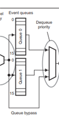
    in your code I see you have used 3 event queues for EDMA, however EDMA only supports 2 event queues, as can be seen from the TRM.

  • Ok. So what is the solution, can you help on how can this be resolved?

  • something like this: 

    App_dmaConfigure(gAdc1DataBuffer, RESULTS_BUFFER_SIZE, gEdmaHandle[0],
    ADC1_EDMA_CHANNEL, CONFIG_ADC1_RESULT_BASE_ADDR, &tccAlloc0, EDMA_TEST_EVT_QUEUE_NO_0);

    App_dmaConfigure(gAdc2DataBuffer, RESULTS_BUFFER_SIZE, gEdmaHandle[0],
    ADC2_EDMA_CHANNEL, CONFIG_ADC2_RESULT_BASE_ADDR, &tccAlloc1, EDMA_TEST_EVT_QUEUE_NO_1);

    App_dmaConfigure(gAdc3DataBuffer, RESULTS_BUFFER_SIZE, gEdmaHandle[0],
    ADC3_EDMA_CHANNEL, CONFIG_ADC3_RESULT_BASE_ADDR, &tccAlloc2, EDMA_TEST_EVT_QUEUE_NO_0);

    App_dmaConfigure(gAdc4DataBuffer, RESULTS_BUFFER_SIZE, gEdmaHandle[0],
    ADC4_EDMA_CHANNEL, CONFIG_ADC4_RESULT_BASE_ADDR, &tccAlloc3, EDMA_TEST_EVT_QUEUE_NO_1);

  • Hi Akshit,

    Here is an Update:

    Just by changing the QUEUE to 0 it did not work. I had to add more PaRAM set in the EDMA Registration code. With this change, I now get data properly for ADC0-AIN0, ADC1-AIN0 and ADC2-AIN0. Ref attached code.

    BUT adding ACD3-AIN0 is not working now, the first 3 adc continue to work properly. I need to add ADC3 and ADC4 to this code. Please review the code and let me know what's going wrong. This is a bit urgent so please help.

    adc_soc_continuous_dma_am263x-lp_r5fss0-0_nortos_ti-arm-clang - ADC0-3AIN0Working.zip

  • Hi Yogesh,

    I don't see ADC3 and ADC4 added to Sysconfig in the code you shared. Could you check for that?

    Regards.
    Akshit

  • Hi Akshit,

    Thanks for the reply. I could modify the code for reading AIN0 of all 4 ADCs (ADC0 to ADC4) and could successfully test. Attached is the code for your review.

    Now I would like to add AIN1 to AIN5 for all these ADC. May I request you to help on this quickly. You can build the attached project.

    adc_soc_continuous_dma_am263x-lp_r5fss0-0_nortos_ti-arm-clang - ADC0-4AIN0Working1.zip

  • Hi Aksihit,

    Now as AIN0 of all ADCs (ADC0-ADC4) are working, I am attempting to add the rest of the channels i.e AIN1 to AIN5 of all the ADCs. Ref attached code.

    But NO SUCCESS yet. Can you help here quickly to fix on what am I doing wrong?

    4520.adc_soc_continuous_dma_am263x-lp_r5fss0-0_nortos_ti-arm-clang.zip

  • Hi Yogesh,

    If the use case is for simulteneous sampling of all 30 channels (6channels (AIN0-5) of 5 ADCs)? then it is not possible, as a single ADC will be unable to simultaneously sample 4 different sample voltages..

    If the use case is for simultaneous sampling of any one channel from different ADCs at any point of time, then it is possible


    AIN0 from all 4 ADCs can be simulteneously sampled
    AIN1 from all 4 ADCs can be simulteneously sampled
    ...
    AIN5 from all 4 ADCs can be simulteneously sampled
    but all of these need to be time multiplexed

    Regards,
    Akshit

  • Hi Akshit,

    Yes, the usecase is to sample all 30 channels i.e All 6 channels (AIN0 - AIN0) of all 5 ADC (ADC0 to ADC5). Expecting it to be samples in round robin not simultaneous. Can you look at the code and let me know where is the issue? Please.

    Can we have a quick call as we are in same time zone.

  • Hi Yogesh,

    1. some other SOC can be configured for a different channel. for ex: SOC1 for ADCIN1


    2. A new buffer to store the values

    3. A new xbar route for the channel 

      #define ADC1_1_EDMA_CHANNEL (DMA_TRIG_XBAR_EDMA_MODULE_10)

    4. Modify the function to accomodate SocNumber. For ex:

      /* Function Prototypes */
      uint16_t App_dmaConfigure(const uint16_t *table, uint16_t table_size,
      EDMA_Handle dma_handle, uint32_t dma_ch,
      uint32_t adc_base, ADC_SOCNumber socNumber, uint32_t *tccAlloc, uint32_t event_queue_number);


      App_dmaConfigure(gAdc1DataBuffer1, RESULTS_BUFFER_SIZE, gEdmaHandle[0],
      ADC1_1_EDMA_CHANNEL, CONFIG_ADC1_RESULT_BASE_ADDR, ADC_SOC_NUMBER1, &tccAlloc5, EDMA_TEST_EVT_QUEUE_NO_1);
    5. Change the srcAddr ->
      edmaParam1.srcAddr = (uint32_t) SOC_virtToPhy((void *)(adc_base+CSL_ADC_RESULT_ADCRESULT0+((uint32_t)socNumber * ADC_RESULT_ADCRESULTx_STEP)));

    Let me know if these changes solve the issue for you!

    Regards,
    Akshit

  • Hi Akshit, Thank you.

    I used the steps you provided and modified the code for all ADCs (ADC0-4) all inputs (AIN0-AIN5). But I get an exception for AIN3 input.

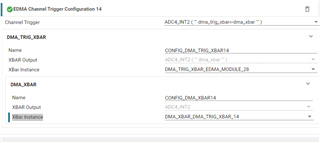
    An observation. In example.sysconf DMA_XBAR can be configured only up to 14, thus AIN0 to AIN2 of all ADCs are working as expected but AIN3-AIN5 are NOT.

    To test. Ref attached code ,I DMA configured only for 3 Inputs i.e AIN0-AIN2 (#define REG_ADC_CHANNEL 3) for all ADC modules and AIN0-AIN2 works as expected. Now question is what do I modify to make AIN3-AIN5 work? Please review attached code and let me know how to rectify for AIN3-AIN5.

    adc_soc_continuous_dma_am263x-lp_r5fss0-0_nortos_ti-arm-clang - ADC0-4AIN0-2Working.zip

  • Hi Akshit,

    Thank you for your support. It looks like ALL Inputs i.e AIN0-AIN5 of all ADCs ADC0-ADC4 are now working. Some of the configuration was missing which I rectified.

    May I request to have a look at attached code and provide your feedback for improvements.

    adc_soc_continuous_dma_am263x-lp_r5fss0-0_nortos_ti-arm-clang - ADC0-4AIN0-5Working.zip

  • Hi Yogesh,

    I am glad the system is working now.

    I apologize for all the inconveniences caused and thank you for providing the final working code.

    I'll review today and get back to you asap.

    Regards,
    Akshit

  • Hi Akshit,

    I tested it again today and looks like all AINs are not converting. Probably I know the reason, but will need your help.

    I think it worked yesterday because:

    -I shifted the XBAR triggers from AIN0-AIN2 to AIN3-AIN5 to test this set. AIN3-AIN5 worked but AIN0-AIN2 did not.

    - Then I shifted XBAR triggers again to AIN0-AIN2, the board was always on thus when ran this code, all AINs of all ADCs were converting data. Probably because trigger of AIN3-AIN5 was done is last run. Later the board was powered off. 

    Today morning I powered on the board and flashed the same code again and only AIN0-AIN2 worked. Looks like yesterday it worked because conversion trigger for AIN3-AIN5 was started and because board was always on.

    Please help to resolve this issue.

  • Hi Yogesh,

    understood, as there are only 16 DMA Xbar channels available, getting 30 ADC channels to work with them simultaneously is not possible.

    The approach that I am thinking of is:

    • to setup a schedule where the second set of ADC channels are read after the first, using the same DMA channels.
    • An interrupt or a timer can be setup to switch XBAR connections whenever one of the two sets completes the transfer. (this switch can be done in the ISR)
    • You can view the XBAR configurations, in .../ti-arm-clang/generated/ti_drivers_open_close.c; functions: 
    • Drivers_dmaTrigXbarOpen()Drivers_dmaXbarOpen() and use the API SOC_xbarSelectEdmaTrigXbarInputSource() to change the source ADC channels.

    Let me know what you think!