This thread has been locked.
If you have a related question, please click the "Ask a related question" button in the top right corner. The newly created question will be automatically linked to this question.
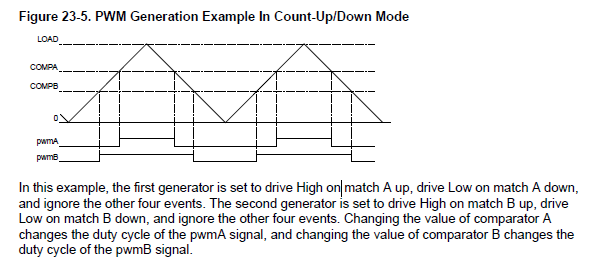
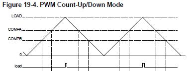
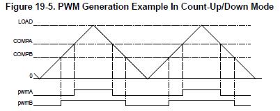
Figure 23-5 below infers there to be only a single pulse on A or B PWM output Up/Down counter mode during load and zero count match. An attempt was made in an earlier illustration of the up/down PWM generator counter to show a reoccurring pulse stream in a very confusing way. A single output pulse from PWM generator A&B is then shown to occur for the zero to zero transition below.
Might the PWM generator A&B output signal be drawn incorrectly in relation to the discussion on the PWM up/down counter mode? Does the PWM generator output only a single pulse for a incremental up/down count of many integers only when the comparators match a set point in the sloping integer count? If so in a 20Khz PWM frequency & resulting trapezoidal wave form a single PWM generator period of integer counts results in a single 50us pulse inside the trapezoidal wave form over 1ms in horizontal length. More over then load count match occurs at the peak of every 50us pulse with (zero) count pulse on either side of each and every 50us generator pulse. Possibly this topic has been over simplified to the point it makes no sense in relation to the Tivaware C++ programming of the PWM generators and other functions. Tivaware is not alone Stellarisware departing with the same diverged datasheet topic to actual occurring PWM events in the real world of DSP leaves one scratching head, beard and or whiskers!
This figure below does not make that point clear as it relates to the resulting trapezoidal wave form or center aligned PWM pulse stream when (pwmA & pwmB) are not shown to have more than one rising and one falling edge. The relation to this diagram and the resulting trapezoidal wave forms (below) figure 23-5 share similar pyramid architectures making a through understating of it even more confusing.
Hi Amit,
Nice try but that does not answer the more pressing questions being asked. When and where comparator matches occur in real time PWM generator output events? Do the A&B generator outputs follow the count up/down exactly or only the comparator match events in building a center aligned PWM pulse stream?
Other words is the A&B signal in Figure 23.5 representing a single PWM pulse or abstracting the entire trapezoidal wave form created from the count up/down matches of theses comparators. The Figure makes no sense in the world of counter theory since an count up/down count includes more than a single BCD or integer transition. Multiple increment/decrement integers would toggle the output more than one time. Figure 23.5 showing only a single rising & falling edge does not properly describe how the A&B outputs would toggle during a count especial since it is depicted with zero(0) and LOAD nomenclature.
More importantly Figure 23.4 & 23.5 failure to illustrate the PWM generator A&B output signal not at all or as a pulse stream is important because the ADC sample triggers can be fired by the PWM generator during any of the 4 comparator, PWM Load or zero events. Thus one has to know where in the resulting trapezoidal wave form the comparator match occur in real time. All figures if kept the way they are would then need to show where the ADC trigger points occur in the PWM generator output pulse. Thus one would not simply deduct the data sheet PWM figures abstracts a Trapezoidal wave form.
BP101 said:When and where do the ADC triggers assert in relation to the A&B output in figure format?
While the MCU manuals may not be "crystal clear" - perhaps this "cut/paste" from hallowed LX4F manual - supplies the "when." Where depends upon the PWM Generator's config. and (likely) the particular PWM modulation scheme. If Trapezoid Modulation & "Slow Decay" is selected - then "only" the high-side PWM driver's reaching its "load value" serves as the ADC trigger. This requires, "PWMGenIntTrigEnable()" with parameter, "PWM_TR_CNT_LOAD." Note that other ADC triggers exist - yet this particular one triggers (as you ask) - during PWM impulse's center.
As that occurs at PWM Center - the ADC Trigger should be proper - even (and especially) during low-duty cycles. (an ADC trigger too early - or too late (as opposed to center of the PWM output) - would likely "miss" a narrow PWM impulse.) That's "le raison d'etre" for "center based" PWM triggers of the ADC...
MCU Manual Extracts - supporting this assertion - follow:
Our small firm also was intrigued by this - we confirmed this "center of PWM impulse ADC trigger" by driving the selected ADC channel input with a ramping, linear voltage - which served to reveal the "very near to PWM center" ADC measure...
Hello CB1,
Was quite aware these points made above. Was actually requesting a figure format clock timing illustration showing the PWM clock pulses and the 6 PWM generated trigger points with respect to comparator A&B outputs.
The defining difference between Load and Zero triggers (data sheet states) comparator A&B match is ignored if ever they occur simultaneously with Load or Zero. It is plausible two distinct pulses of the trapezoidal wave form generation might actually trigger undesired current samples during Load match. This symptom is hard to unravel not knowing where the comparator match count to ADC trigger points occur in relation to the pulse period. One can only use visual feed back from test equipment to determine what and why.
BP101 said:Hard to imagine comparator match ADC triggering being any less edge aware than Load match no matter the PWM pulse width.
Edge awareness impacts (other) than the "TRCNTLOAD" ADC Trigger I referenced. Review the "Center based" ADC Trigger (diagram, below) - note the load pulse is "dead-centered" w/in the PWM impulse (either of them)!
When the PWM pulse width is short - which results from low duty cycles - the importance of such, "Trigger on load" becomes especially magnified. While there exist 4 "comparator edge" ADC triggers - each/every one exist at the (very) beginning or (very) end of the PWM impulse - and an ADC trigger at such extreme seems "less effective" than "Trigger @ PWM Center."
Power Engineering texts detail very well - if I may recite their "essence" - "ADC Triggering as a pulse just begins" (counting up) may be too soon - may miss the peak current. (expected close to center) Likewise - "ADC Triggering as a pulse just falls/extinguishes" (counting down) may be too late - again may miss the peak current. Again - this is not my invention - I'm simple recipient/exploiter (ot text's valued guidance) & reporter, here.
Center based triggering is employed by all such MCU vendors - and was used in the days of "dedicated" BLDC Controller ICs (prior to MCUs) - as well.
As duty cycles "flirt" w/90%+ the requirement for such "dead center ADC Trigger" may lessen - and one expects that's what you're reporting.
That said - "center based ADC trigger" has long been proven - we'll (and many/most here) will continue in its use & application...
BP101 said:That's a far stretch to say when in fact the comparator match points are not at the very end according to figure 19-4
My friend - one (crystal clear picture = 1000 words! Look (instead) here: Fig 19-5: (one diagram further than your 19-4!
Your use of "far stretch" to attack your "helpers" is curious - is it not? And earlier - your response to Amit's writing - was, "Nice try!" That's not right nor proper!
Rather clearly - when "up counting" an ADC Trigger is delivered (just as past stated) at the very beginning of the PWM impulse. When "down counting" the ADC Trigger is delivered (again just as past stated) at the very end of the PWM impulse. There is absolutely "No stretch" yet alone a, "Far stretch" to note.
Why do you characterize this as a "far stretch?" PWM impulse (either of them) commences EXACTLY @ the match point - and extinguishes EXACTLY @ the opposite match point!
Earlier - my (unverified) initial post - I described (rather exactly) "how we'd know (exactly) where the match points could be determined..."
I'll leave to Amit to detail fig 19-4 - which serves a different role - due to its use of "direction." Hopefully his explanation may escape, "stretch!"
Let me register vote #2 for, "Not confusing!" One hopes your writing (this time) does not warrant a second, "Nice try!"
Hard to understand how (would be) helpers warrant such stern rebuke. Just two have responded - might there be a reason?
Earlier - my (unverified) initial post - I described (rather exactly) "how we'd know (exactly) where the match points could be determined..."
Was referring to the ramps (^) in the count positions match points and actual location in the resulting trapezoidal wave form are not exactly at the beginning and ends of a single pulse period. For one the MOS free wheeling diode in the high and low side FET shuts off at the down count ends of pwmA&B causing a ringing in the signal that extend beyond down ends period timings and flowing into dead band.
The inductive phase coil voltage also hangs around for a while longer after the FET shuts down. Hence the current lags behind the voltage beyond the trigger point of a center sample. A 4us center sample just barely catches declining current ramp, speaking of each individual low side phase current not the total high side B+ source return a current (probe) my reveal. Since horizontal time base is moving from right to left the current sample points can best be witnessed; Scope triggering set on the trapezoidal wave form (voltage) order to see inductive (current) lag behind the trigger points.
Simple figures as clarification get fuzzy upon trying to back step into the trapezoidal signal build. Becomes difficult to visualize pwmA&B when trying to mentally set imaginary ADC trigger points within the resulting trapezoidal and current wave form. Only then do we know without doubt the ADC triggers are asserting exactly as they are programmed to and sampling in the ideal time position.
However appreciative in each every response there lacks the answer for trapezoidal wave form timing material being asked for in the 1st and later posts. Apologize for any perceived frustration my part alone is enough head explodes leave white walls grey matter soaked.
Obviously the first in kind a tagged scope capture below attempts to clarify why the timing of the comparator edges is so vital from the stand point of where Zero and Load match logically should occur in the trapezoidal wave form. The PWM clock pulse missing from all figures makes it difficult to know where the hard edges might occur from the data sheet text alone. Least of all the electrical specifications make no attempt to air any such similar laundry.
Two wave forms superimposed saw tooth current pulses inside Trapezoidal PWM (Illustrate) where ADC trigger points logically should start/end each PWM pulse and trigged ADC sample period. Suspecting the advantage of using comparator B down to trigger current sample is the fact a Zero or Load match occurring simultaneously will Avert taking a current sample when I suspect the duty cycle falls to zero anyway. Like wise if BEMF is being sampled with the same ADC trigger a concurrent Zero or Load during Comparator B down should avert taking any would be false zero crossing samples. Like to have others do similar test and report the results in scope captures. Possibly TI can generate a Wiki paper of some kind?
Current envelope (top trace), Free Wheel diode ringing pattern at the end of each PWM pulse period (bottom trace)
"use this to change one of the comparator threshold"
Might this be ADC differential mode you are referring as the comparator threshold?
The configuration being described samples single analog input mode, 3 inputs 1 for each leg of the bridge.
The electrical characteristic section of datasheet TM4C1294NCPDT list ADC latency 2 ADC clocks = (125ns), (Ts)= 250ns sample time, (Tc) 1us conversion @1Msps. Setting ADC hardware averaging 32x divides (Ts) 250ns, rending a (Ts) 8us sample plus 1us (Tc) = 9.375us total yet still an incredibly short time. Believe the sampling capacitor formula adjusts the ADC internal sample hold period based on the expected analog input resistance is omitted from the electrical section and is waiting for update in 2Msps electrical section?
Now sampling with ADC inside LM3S8971 MCU - ADC Now have over sample 32x= (Ts) 9.4us is capturing current rising slope @match CMPB down. The ADC now samples for three very precise INA282 shunt monitors on the low side MOS. Possibly the TM4C1294NCPDT ADC phase control time delay can be of help for insisting center trigger-errs? A time phase delay added to ADC1 after the PWM Load match trigger might actually catch rising current peaks instead of my perceived falling envelope.
Amit Ashara said:it has to be kept in mind that the ADC will sample the data after resynchronizing the PWM trigger to it and then start charging the Sampling Cap for 4 clocks of 16MHz
Hi Amit,
I blew up that portion of your explanation which is "outside my knowledge." We know that sometimes you're forced to write "fast-furiously" and the writing I've highlighted seems to grant (at least to me) "NEW POWERS" to the ADC! I was (and remain now) "unaware" of the ADC's ability to "Resynchronize any PWM Trigger!"
Would not any such "resync" of the PWM Trigger by the (pardon) lowly ADC - "throw into ruin" the entire concept (at least a substantial part of same) of PWM Triggered ADC measurements?
We know that multiple, PWM Generators are often "Sync'ed" and the MCU manual explains that process as intended to prevent, "ill formed PWM pulses." That said - never/ever - here or w/in multiple other ARM MCU manuals - have I read of the "ADC being able to "boss/control" the PWM Generator."
Would you be so kind as to give a quick read/review of that past paragraph - and then confirm/deny - the ADC's "resync" of the PWM Trigger. Should you verify this - does it appear anywhere where we "mortals" (w/out regular/serious access to "insider info) may read in some detail?
Thanks your time/attention...
"The PWM works in System Clock Domain (and add to that the divider options) while ADC is fixed 16MHz clock domain"
Regards to the TM4C1294NCPDT; Does not the ADC (sample clock) run at 1 or 2 Msps derived from a divided SYSCLK only for sampling. The 480mHz PLL/30 MOSC clocks the ADC peripheral @16mHz for conversions and data across the peripheral interface onto the local bus but not for sampling or triggering sequencers.
My take on ADC trigger based on data sheet TM4C1294NCPDT is ADC trigger always runs synchronous with PWM:
The PWM peripheral runs from divided SYSCLK to generate a 60MHz PWM clock same SYSCLK for ADC sample clock. That said, the PWM generator triggers the ADC channel sequencer ADCEMUX to enable sampling and runs synchronous by rule of same clock source. It doesn't add up the ADC sequencer or trigger running at ADC peripheral clock speed 16MHz when sampling is far slower at 1-2 Msps filling the sequence FIFO at the sample rate and or constrained by hardware averaging.
"The only thing being maintained is the phase of rising edge on the slow clock from the fast clock"
Ok - yet in this case SYSCLK is used to clock both peripherals in regards PWM to ADC trigger and sample sequencer. Again one might deduct there should be no discontinuity between the PWM and ADC peripheral trigger edge timing or perhaps not.
Seems like your inferring there to be issues in the clocking of FIFO data onto the local bus when the 16Mhz ADC clock skews apart from SYSCLK the sample sequencer is delayed by up to 1 SYSCLK before acting on the PWM trigger. The ADC then sets a trigger wait state on the sequencer array delaying 1 SYSCLK before acknowledging the request to the PWM generator and waiting until both clocks are again synchronized to finally process that request?
Good question you knew I was going to ask: How often does SYSCLK skew occur and can it be mitigated by software in some way?
Like this new feature of TM4C1294NCPDT ADC: Busy Status
The BUSY bit of the ADCACTSS register is used to indicate when the ADC is busy with a current conversion. When there are no triggers pending which may start a new conversion in the immediate cycle or next few cycles, the BUSY bit reads as 0. Software must read the status of the BUSY bit as clear before disabling the ADC clock by writing to the Analog-to-Digital Converter Run Mode Clock Gating Control (RCGCADC) register.
Thanks Amit,
Something more profound came out this thread. TI could add an ability to set a number of peripheral clock wait states after the PWM generator triggers ADC, lagging behind the sample time. Setting the ADC hardware averaging 32x just to capture a small portion of what may not be even the average is troubling. Suspect 32x sample time (9.4us) might possibly interfere with the minimum pulse width constraint low (.5us) when triggering ADC sample on PWM generator comparator B down.
3/5/2015 Setting ADC sample trigger match comparator B down interfered with sensorless commutation also being in the same sample as current measure. That results in crashing the commutation timer on very rapid motor acceleration and shoot through occurs every single time.