This thread has been locked.

If you have a related question, please click the "Ask a related question" button in the top right corner. The newly created question will be automatically linked to this question.

EK-TM4C1294XL: ADC Bandgap reference

Guru 54808 points
Part Number: EK-TM4C1294XL
Other Parts Discussed in Thread: TL081, LM741

Does the ADC have a 1.65v bandgap internal reference for full scale VREFN  and VREP +3v3 for channel set to single ended input mode?

What is the benefit of 1.65v band gap internal reference, if not existing do the samples near mid VREFP become error laden?

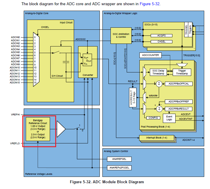
This ADC module below used by other TI engineers to determine mid VREFP sensor functionality for all SAR type ADC, seemingly problematic for TM4C1294. 

When a 1.65V internal reference voltage is selected, the effective ADC conversion input range will be VREFLO to 3.3V.

  • Hi BP101,

      Where did you find the block diagram?

  • Compare above ADC to TM4C1294 ADC questionable VREFA+ may not power converter directly from VREFP?

    If actually TM4C1294 AD converter sources 3v3 from VDD rail and NOT VREFP then VREFA+ powered +1.65v external reference may be required for fixed mid VREFP analog input signals to properly converge? How could the theory behind these ADC modules be so different in band gap aspect or converter method?


  • Hi Charles,

    That is one of TI Other MCU embedded ADC's modules. As Bob was informed the step approximation granularity from mid VREFP was producing large steps +/-100mV Peak from fixed midpoint (1.65v) input convergence. A scope widget plotted visual magnitudes act like the internal reference (3v3) is double what it should be for fixed center input sample.

    That internal 3v3 reference seems to explain why the FIFO values quickly peak from very small input changes around a fixed center input 1.65v. Can you confirm that is the case for why the FIFO values would be much greater (coarse granularity) than those samples from VREFN-VREFP and the same internal reference 3v3?

  • Hi Charles,

    I was seeking confirmation if +VREFA electrical specification is made < +2.4v, will the converter still work? Seemingly this sensor works with ADC band gap (+1.65v) to produce mid VREFP with even full scale granularity. The TM4C129x ADC seems not to produce the same linear results above 2048 @1.65v relative to VREFN - VREFP samples derived from the same sensor. Those latter samples are fairly consistent but from mid VREFP make no mathematical sense. Yet sensor forum claims it works with SAR, via similar testing done via C2000 ADC, above diagram.

    The TM4C1294 linear conversion results for this sensor changes dramatically from ADC full scale and switching to mid VREFP full scale modes. Seemingly the sensor linearity does not change between modes or is compensated for certain ADC modules.

    The converter guard band may some how compensate for analog signals fixed center @1.65v, seems an reasonable explanation does it not?

  • Hi BP101,

    Gl said:
    I was seeking confirmation if +VREFA electrical specification is made < +2.4v, will the converter still work?

      The min voltage for VREF+ is 2.4. You cannot go below 2.4V.

  • I can read too but can you confirm it to be true using a launch pad or even researched the converter design of this ADC? FE has to question where on earth 2.4v Min came from if internal converter supply is tied to VDD 3v3 or LDO 1.2v which is it? Surely the converter is not tied to VREFA+ via VREFP switching. Something is not adding up here these two ADC can be so different from the same manufacturer. Companies licensing silicon into USA markets, past time to end that trap! 

    I'd rather not burn up this launch pad in the process of getting an answer to easy question the FE should have access to the answer. At least testing VREFA+ 1.65v it could aid in determining digital scale 0-4096 remains consistent. 

  • According to this article link, analog input signal "centered(fixed) mid VREFP" (+1.65v) is neither unipolar or bipolar. By ADC analog channel input definition in (link) such fixed signal does not exist! 

    Yet the "fixed mid VREFP" analog input creates fictitious mathematical zero crossing events well above ground, VREFP-2048 or (+1.65v). And is not a unipolar analog input signal since it attempts to divide actual zero crossing events from a fixed baseline (1.65v). However the real DSP events being converted to lower analog converter levels do not ever zero cross and originate from a single ended power source.

    WiKapedia has no clarification for a centered analog signal of this kind existing above ground. Yet TI has developed several components that replicate artificial analog zero crossing events well above ground and no examples of how SW is able to decode such samples. Example: A device sources 20 amps from a DC power supply,e.g. Does it actually source the same positive as negative current relative to ADC full scale (0-4096) just because the amplifier converts ground level artifacts in this fixed VREFP way?

    Do we simply dismiss DMM digital readout produces a positive sign with minimal decimal changes being the +/- sign never toggles on the LCD display. It would seem TI datasheet text has bamboozled the community into believing bidirectional monitoring is possible via sensors placed on low side of DC inverter. That forum repeatedly skirts truth low side sensor placement does not properly work fixed mid VREFP (1.65v) via the TM4C1294 ADC module. Forum gurus never examine why or how sensor fails with TM4C SAR ADC. However earlier TI bidirectional amplifier designs disprove certain claims of new sensor datasheet and forum gurus maintain unprecedented stance even when presented with a contrasting view. 

    https://www2.advantech.com/ia/newsletter/ADAMLINK/Oct2005/IO1.htm  

  • Charles a good read of what band gap does for ADC.

    The band gap reference theory has an early Analog Devices beginning.

    https://wiki.analog.com/university/courses/electronics/text/chapter-14#bandgap_references 

  • Hi BP101,

     Thanks for the link. 

  • Hi Charles, 

    Who'd be the wiser Brokaw cell band gap reference theory goes back to 1974. Issue reminds me StarTrek Captain Piccard faced with aliens knowledge of existence, could not allow ship being stuck in space time loop (memories wiped) kept traversing back to get answers "why, how, where" otherwise be extinguished by these aliens.  

    One logical explanation; internal VREFP derived VREFA+ becomes partially saturated 1.65v via analog signals 2 other AINx inputs centered mid VREFP (1.65v), total of 3 inputs.

    Perhaps why converter can not produce samples ≈100mv above or below (VREFP) band gap reference (1.65v) relative to count 2048. Even thought the external signal magnitude changes >1.75v+- the converter section does not see any analog difference and produces 0µV step approximation. There is little datasheet discussion ADC internal VREFP or how it mitigates noise so well but it does a good job in that aspect!

    The original sensor WA being (VREFN-VREFP) no saturation of 3 AINx inputs seems to occur 240us sample intervals. Ideally like to sample sensors <240us but the results tend to be less accurate as noise increases. Does reprogram of sequencer steps each cycle switching among AINx 3 sensors help to reduce internal channel saturation of VREFP centered (1.65v)?  

  • No answers?

    So 3 AINx signal inputs are actively sampled via sequencer steps 0,1,2,3 END IE.

    The problem being several milliseconds of dead signal time any 1 of 3 SSn steps stays fixed 1.65v, saturating all steps of sample hold window. Other sequencer AINx analog signals remain below 2048 counts. They exist in different SSn sample window unaffected by hold saturation of other SSn window. 

    Seemingly band gap accounts for times when analog signals 2048 region guard against zone crossing saturation and temperature drift.

    Datasheet implies isolation exists between AINx channels but does not isolate SSn steps during Nsh/TshN encoding. It would seem multiple steps sharing the same sample window are prone to hold saturation in the band gap region when the analog signals mirror it's bias voltage, 1.65v.

    Seemingly splitting analog signals centered 1.65v is a bad idea relative to ADC sample hold band gap combinations.  

  • Hi BP101,

      I don't know how to answer your question. I will see if Bob can help answer your question. 

      Did you try to increase the S/H window? What differences do you see?

      Can you tabulate your conversion results for the three AINx inputs (all fixed at 1.65v) in different SSn and in different S/H window sizes? I think that will clarify what problem you are seeing. 

  • Charles Tsai said:
      Can you tabulate your conversion results for the three AINx inputs (all fixed at 1.65v) in different SSn and in different S/H window sizes?

    The 3 samples have to exist in the same SSn. At one point SW reconfigured single step SSn each AINx, that method was oddly omitting samples via 25µs IE. The S/H has no effect, sample window is very wide already >240µs versus 25µs. That was why to question if external reference 3v3 and mid VREF also affects launch pad fault comparators internal resistor ladder threshold. 

    The easy answer being amplifier must be configured to produce analog signal that does not adversely affect conversion. The closer to ground signal originates more accurate conversion results. Seems it was unknown ADC gap band can be effected via split signal in 2048 count region. That split analog signal AINx current perhaps swings two directions causing region saturation. That was one reason to consider external REFA+ may not have this same cause and affect as does the internal VREFP reference. 

  • Gl said:
    Does the ADC have a 1.65v bandgap internal reference for full scale VREFN  and VREP +3v3 for channel set to single ended input mode?

    No, the diagram you posted is from a different device.

  • Bob Crosby said:
    No, the diagram you posted is from a different device.

    How do you know that to be true as most every ADC produced since 1976 include band gap counter measures in order to reduce precision losses due to silicon temperature changes?

    It seems the 3 analog signals produce AINx current reversals during bottom 1/2 crossing, 90° out of phase from top 1/2. Some how calibrated full scale reaches roughly 75mV above mid VREFP (2048 count) refusing to count higher or lower even though the the three AINx inputs can easily be made to exceeded the original magnitude >1.725mV. The software algorithm stacks ratio metric slope changes relative to digital slope in either sensor mode.   

    The AINx analog input current swings nearly equal in opposite direction upon crossing mid VREFP.  When AINx analog signals originate (VREFN-VREFP) and not being split mid VREFP (1.65v) the results ARE superior. Yet the sensor datasheet graphs do not indicate output linearity changes relative to either configuration. That seems to imply the 3 sensors signal somehow produces damaging artifacts that affect ADC 1/2 scale (2048) calibration relative to VREFP internal current source.....  

    1. How are the internal ADC 1/2 scale (2048) so easily being inflicted by INAx analog current reversals? 

    2. Will an external VREFA+ precision 3v3 reference counter measure 1/2 scale saturation as above described?

  • Gl said:
    How do you know that to be true

    I work for Texas Instruments and have access to the internal design. It is a ratiometric successive approximation analog to digital converter. 

    You keep contending that there is an issue with the ADC on the TM4C1294. No one else is having the problems that you are having. I suspect it is a system problem. I asked in the previous thread if you would provide a schematic of your input signal. You have chosen not to. I am honestly not sure how to help you.

  • Bob Crosby said:
    I work for Texas Instruments and have access to the internal design. It is a ratiometric successive approximation analog to digital converter. 

    Agree but that is saying nothing the Analog Devices article states band gap exists in most analog devices like the C2000 ADC shown in very first post.

    Bob Crosby said:
    You keep contending that there is an issue with the ADC on the TM4C1294.

    I have recently confirmed ADC has odd clocking skew relative to PWM clock division, producing 60Mhz PWMCLK. The 120Mhz ADC (32Mhz sample 2MSPS) is skewed by several hundred SYSCLKS 6400 ADCCLOCKS. Perhaps causing some of the issue with acquisition via PWM generators, ADC trigger source thus produce incorrect digital values since the acquisition window is not where it is supposed to be, e.g. PWM_TR_CNT_LOAD via 1st generator. 

    A new work around required PWM_TR_CNT_BD placed on very last generator of 3, versus PWM_TR_CNT_LOAD 1st generator. Yet even that according to external test equipment produces >38% low end error where only 2% should ever exist. Comparator _BD is the very last count event that occurs capable to trigger the ADC at the 2x PWM period Nyquist rate. Otherwise we have to fire a GPTM one shot triggering ADC sequencer 240µs blanking intervals order to remove excessive low end error % and improve the high end acquisition.

    The take away being synchronous ratio metric digital slope is achieved via PWM_TR_CNT_BD not PWM_TR_CNT_LOAD telling us there is an ADC clocking issue. 

  • Gl said:
    The take away being ratio metric digital slope is achieved via PWM_TR_CNT_BD not PWM_TR_CNT_LOAD telling us there is an ADC clocking issue. 

    Anyway TI senor (attached pdf) replacing discrete amplifiers (below) produces different analog signal seems part of the issue. Discrete amplifier inverts input so 1/2 analog sample is missing via SAR compatible TI sensor. Obviously TI sensor is not exactly compatible since the ADC acquisition window is severely shifted into PWM_TR_CNT_BD of 3rd generator versus PWM_TR_CNT_LOAD 1st generator. And even that phase shift being partly accounted for (_BD) is not acquisitioning the analog envelope at the correct time via PWM triggering. GPTM oneshot 240µs triggering ADC conversion seems to reduce the error % but no where close to the precision values listed for the sensor SAR acquisition. So the expected sensor precision is no where close to what the SAR is acquisitioning for the signal being generated.

    /cfs-file/__key/communityserver-discussions-components-files/908/Total_5F00_Error_5F00_vs_5F00_Sensed_5F00_Current_2D00_-0.5A_2D00_50A-2mOhm.csv

    Schematic: /cfs-file/__key/communityserver-discussions-components-files/908/INA240x3-Experimental-Schematic.pdf

  • I think you have wandered from the original question. The original question was if the TM4C1294 device uses a bandgap in the ADC. The answer is no. Statements by Analog Devices do not apply to Texas Instrument's parts.

    Next you claimed the ADC was not converting properly near the mid reference (1.65V) range. Has that claim now been dropped and replaced with the claim that the ADC is not sampling at the correct time? How do you trigger the ADC? Do you have each motor phase on a separate ADC sequence?

  • Bob Crosby said:
    Next you claimed the ADC was not converting properly near the mid reference (1.65V) range.

    Yet another part of the experiment producing inaccurate results.

    Bob Crosby said:
    Has that claim now been dropped and replaced with the claim that the ADC is not sampling at the correct time?

    That is the perception since the error count is excessive compared to the calculated and predicted sensor precision via SAR. It would be highly misleading for TI precision analysis calculator to predict sensor precision without the claimed SAR conversion being any part of the predicted precision aspect. What would be the point of predicting sensor precision based only on it's science controls without the intended conversion interface (SAR) being accounted for in that precision formula? Yet seems to be what has driven precision sensor claim of being SAR compatible into the dirt. 

    Bob Crosby said:
    How do you trigger the ADC?

    As later explained each experiment tested 2 acquisition trigger windows in order to achieve the highest precision possible via two specific sensor modes. Neither mode produces precision sensor analysis predicts via SAR conversion results. And only later to read/understand sensor randomly phase shifts output relative to synchronous acquisition triggered window. Seemingly accounts for GPTM trigger source producing finer granularity results via 240µs sample window versus 25µs trigger source.

    Also reading yesterday high bandwidth discrete amplifiers account for input overshooting +/- rail thus reduce chances of phase shifted output. Reason why TL081 Fig.8 graph showing 90° output phase shift occurs in a certain frequency range of bandwidth! Sensor band width (350Khz) compared to discrete amplifiers (3Mhz) shown in above posted schematic. Tested sensor claims of SAR compatibility do not live up to application via TM4C1294 12 bit ADC ability to easily acquisition phasing moving input targets. Perhaps the most plausible explanation why the SAR conversion granularity suffers as it does via these sensors.

    Bob Crosby said:
    Do you have each motor phase on a separate ADC sequence?

    That would not be very prudent nor possible and only one sequencer is triggered for 3 analog inputs. 

  • Bob Crosby said:
    . The original question was if the TM4C1294 device uses a bandgap in the ADC. The answer is no. Statements by Analog Devices do not apply to Texas Instrument's parts.

    Again the C2000 SAR 12 bit ADC does incorporate Band Gap (1.65v) internal reference as shown in very first post. It would seem this is a necessary part of TM4C1294 internal VREFP 3v3 reference or the results would stray greatly with ambient temperature changes around the MCU. You offered no explanation of  how ADC stability is being achieved by TM4C1294 internal VREFP reference. The single word No is hardly an answer as to how said stability occurs without band gap referecne. Analog Devices is not the only company using such band gap reference theory! 

    Bob Crosby said:
    I think you have wandered from the original question.

    This thread post a related question and was still not fully answered for the original question. "Why sensor has excessive SAR acquisition issues in any modes being configured TM4C1294 ADC" It would seem TI expects customer to do full investigation when engineering issues are often device related and no followup resolve ever occurs after posting numerous encountered issues relative to a specific device. 

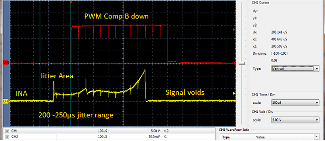
  • The sensor analog signal seems to phase shift asynchronously for the synchronous ADC triggered events. How was phase shift not ever mentioned or even noticed by the engineers in sensor department? Once again captured analog signal via two different digital oscilloscopes and eye witness random rapid phase shifting relative to the synchronous ADC time base as scope trigger source. Note how the signal (CH2) shifts left where last few peak current PWM cycles (CH1) are void any analog signal. That often happens both directions from center COMP_BD and explains huge ADC sample error being produced from multiple sensors. 

    How was device properly tested by TI to confirm consistent sensor behavior across lots persists? Perhaps laboratory did not check input to output phase relationship or offer any graphs to indicate to what degree counter measures even exist. The SAR ADC in this case expects the sensor remain synchronous to the PWM triggered ADC time base, which it does not at all times achieve. Noticed this shift on occasion and simply did not put it together expecting the forum experts should know best. 

  • Gl said:
    How was phase shift not ever mentioned or even noticed by the engineers in sensor department?

    8.3.1.2 Input Signal Bandwidth
    The sensor input signal, which represents the current being measured, is accurately measured with minimal disturbance from large ΔV/Δt common-mode transients as previously described. For PWM signals typically associated with motors, solenoids, and other switching applications, the current being monitored varies at a significantly slower rate than the faster PWM frequency.

    Note: TL081 datasheet shows graph (Fig.8) where a 90° output phase shift occurs for large frequency CM input signals. The ADC sample widow may not entirely frame or follow a phase shifted signal no matter the RS impedance or acquisition time of even a mid supply analog signal.

    Some in this forum may not agree with 8.3.1.2 as the above signal capture seems to counter statement as large phase shift seems the bigger issue.

  • As mentioned on page 1064 of the datasheet, the reference is created from VDDA or VREFA+, both are external pins. The accuracy of the reference is the accuracy of the voltage on the chosen reference pin. There is no bandgap used as a reference. If you don't believe me (and you clearly don't,) try converting at fixed voltage near the mid point using VDDA at 3.0V and then again at 3.3V. You will see that the digital result returned will decrease because the fixed midpoint voltage is a smaller percent of 3.3V than of 3.0V. (Hence the term ratiometric AtoD converter.)

    Fortunately your latest scope picture shows that your issue is not an issue with the TM4C AtoD. To be honest, I have no idea how you created a current that turns on before the PWM goes high and turns off before it goes low. My best guess is that you are comparing the current of one phase of the motor and the PWM of a different phase. You cite the figure 8 of the opamp datasheet showing the differential voltage amplification and phase shift vs. frequency. This is an indication of the stability of the opamp, not an indication that your signal will undergo a phase shift. The opamp will be stable at frequencies where the differential gain phase shift is less than 180 degrees, or for this opamp, stable up to over 1MHz. To understand the lag caused by the opamp, look at the slew rate figure 14. The expectation is a time lag of less than 1uS. If you want more information on the opamp, I would be glad to transfer you thread to that group, or you can start a new thread in that forum.

  • I changed the post link to TL081 day ago as LM741 did not have Fig.8 phase shift referred to in post. My last reply evaporated into thin air upon clicking reply button

  • Also tested adding phase delay to ADC1 trigger source PWM gen 3 COMP_BD but random 200µs phase shifts amount to 6400 ADC clocks * (31.25ns). Tested several delay times and only achieved a marginal improvement from the ultra precision sensor uni-direction configuration. And the bi-direction samples mid VREFP (1.65v) was easily 10x less precise as counts quickly go flat after reaching very low steady state magnitude.

    ADC0 is triggered from PWM Gen 1 sets synchronous ADC clock threshold for ADC1 to delay. 

    /* ADC1 has 45° phase delay from ADC0 */
    ADCPhaseDelaySet(ADC1_BASE, ADC_PHASE_45);

  • Bob Crosby said:
    I have no idea how you created a current that turns on before the PWM goes high and turns off before it goes low.

    CH2 is randomly phase shifting left from CH1 trigger source and even truncating 50µs periods at times. CH2 will rise some what relative to CH1 high signal and often aligns directly under CH1. CH1 represents 95% PWM duty cycles low side gate drive. The capture is achieved via scopes ALT trigger function allowing as I understand independent triggering of each channel. So CH2 trigger is not tied directly to CH1 time base, as does Single trigger mode forcing a trigger from the same time base. 

    The idea is to witness external time discrepancy between channels where Single trigger mode reacts only to the rising or falling edge via the same time base. Dual time base scopes are synchronous channels samples from what I have read. So independent sample channels can indicate more exact time information of the external signals. In this case it appears to be random phase shifting of the entire signal. Another older digital scope was used to check the same conditions, CH2 triggers after CH1 mode. Capture below indicates truncation CH2 of the first few periods in CH1. The same phase shift condition capture above post also occurs on this older dual time base digital scope.

  • The point being something between the TM4C1294 and ultra precision sensor occurs that neither forum has or is willing to considered. 

    When the two devices are put into the same circuit they both are being effected in an odd way. The ultra precision sensor 40mV/A output CH2 should be indicating 0A - 10A peak just before the output shuts off.

    Yet the source is only 1.6A and ADC samples must be calibrated by dividing 4096 by some arbitrary number to factor down the last peak. First of all the last rise periods are overly amplified when connected to TM4C1294 analog inputs. Even with Rs = 4K7 and NSH hold where TSn encoding = 0x2 or even 0x4 the impedance match is close, not exact. Pushing the TSn value 0x6 Rs=-9K6 the samples have no 4096 scale resolve, go flat line. If you ever watch 911 or other medical TV shows you know flat lining a signal infers the subjects death.