This thread has been locked.

If you have a related question, please click the "Ask a related question" button in the top right corner. The newly created question will be automatically linked to this question.

MSP430FR2672: Shield for self capacitance slider and very long slider length

Part Number: MSP430FR2672
Other Parts Discussed in Thread: OPA354, , OPA356

Hello,

I am working on a project that requires a circular slider with a total circumference of  nearly 1m. The biggest issue this is parasitic capacitance on this design. For this reason another engineer choose to utilize multiple MSP devices to break the slider up into 5 ~250mm long sliders. Each is controlled by a single MSP. While this reduces parasitic capacitance, it results in 5 different MSPs all operating out of sync. I see two paths forward here:

1. Synchronize all MSPs of a single external XTAL, and provide a sync signal between all MSPs. This would allow us to implement TDM where each MSP samples their given touch slider during separate time slots. Is this feasible or advisable? If all MSPs are synchronous could all MSPs scan during the same synchronous time slot?

2. Switch to using a single MSP with 16ch assigned to 4 slider elements. The max trace length could be up to 500mm long. The parasitic capacitance of this would be massive, and we would pick up significantly more LED PWM noise.

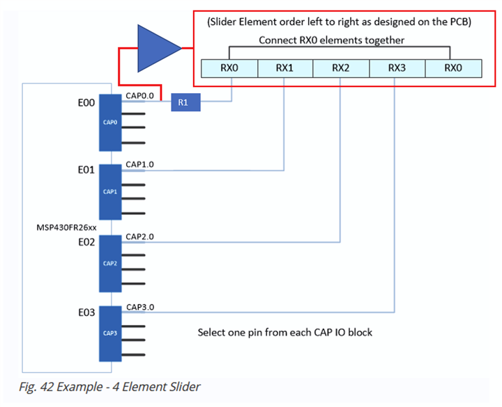
I am also interested in implementing a driven shield under each slider. Currently we are using self capacitance, so I would utilize the OPA354 to drive a hatch plane under slider element. The OPA354 would be connected to CAP0.0 before the series resistor feeding the RX0. Would you please confirm if this is the correct implementation?

Would it be beneficial to tap off CAP2.0, as it has the shortest trace length and lowest parasitic capacitance instead of CAP0.0 that has the longest trace length and greatest parasitic capacitance?

Please let me know if we are barking mad. . .

  • Hi Adam,

    Intriguing! Yes, you are correct about the parasitic capacitance and using a driven shield will help, but with only the one OPA354 driving RX0 won't do the job you want.  The reason is the OPA is used as a buffer amplifier, reproducing the exact same voltage as it's input, right?  In what you are suggesting by the illustration, the voltage on RX0 will appear on the OPA output and drive the shield to same voltage.

    However, there is no guarantee that the voltage on each RX pin will be exactly the same as RX0.  Let's say there is 10mv difference between RX0 and RX1, then RX1 will have a 10mv difference between it and the shield.  And since Q = CV, a small charge will be developed between RX1 and the shield reducing the shield's effectiveness. If there is minimal and equal capacitance on each RX pin, then more than likely driving just RX0 will work well enough to shield all the other RX pins.

    But, since you are driving potentially very heavy capacitive loads that may vary on each RX pin and you have a 470 ohm resistor (for ESD purposes) in series with each electrode, you have a nice RC filter with a potentially slow rise time.  The problem with this is not so much the slow rise time, rather each RX electrode may have a slightly different RC time constant and thus the voltage on RX1, RX2 and RX3 may not track along with the OPA output.

    One more thing to consider is the OPA's ability to drive a heavy capacitive load.  Here is an example of and RX pin (violet) and the OPA output (yellow).  You can see how the output of the OPA could not track the RX pin perfectly.  In all fairness, this photo was not using an OPA354, rather a lower band-width OPA to demonstrate this issue.

    Regarding the solution to use 5 MSP430's, I would tend to agree that might be the better way to go.  You don't need to synchronize the clocks, however, to get all the MCUs to measure at the same time.  There is a pin on the MSP430FR2672 named SYNC.  Typically used for zero crossing in an AC circuit, you could use this pin to trigger all the MCUs simultaneously.  One way to do this is make one of the MSP430s the master and use a GPIO pin connected to it's SYNC pin as well as the other 4 MSP430s and use a timer interrupt to generate the SYNC signal.

    Here are the specifics.

  • Hello Dennis,

    Thank you for the detailed response. The synchronization seems straight forward conceptually. We will see how the implementation goes.

    It is also my understanding that touch performance is typically much better when running off of a XTAL instead of the internal RC. Do you have any information on what impact the clock has to SNR?

    With regards to the driven shield, I understand your comments about the waveform of the driven shield and captivate RX pin not exactly lining up. However, due to design constraints I cannot exactly afford to have a dedicated opamp for each and every RX pad from a quiescent current load or a cost standpoint. Would it be a better strategy to use a single opamp per Cap IO Block, or use additional pins on the MSP to drive a single shield per RX pad?

    The capacitive load for the shield will always be greater than the capacitive load of the RX pad. Thus the shield will always be slightly slower than the RX pad. Could I place a series resistance on both RX pad and shield, and then tune the series resistor on the shield so that the RC time constant is ~ equal for both shield and pad?

  • Hi Adam,

    Whether you use a XTAL or the internal DCO, neither has anything to do with the Captivate performance or SNR.  Reason is the Captivate peripheral has its 16MHz oscillator that can be scaled down to meet the conversion frequency requirements and has nothing to do with the oscillator or clock system on the MSP430.  Captivate also has its own LDO (1.5V) so the analog for the signal chain is isolated from VDD.  

    Keep in mind that Captivate uses a charge-transfer mechanism and clock accuracy has nothing to do with the accuracy of the measurements.

    Regarding the driven shield, typically there is only one OPA and is used to shield a single RX proximity electrode, not on multiple RXs, for that reason.  You would need lots of OPA's, one for each RX channel, to do correctly.  Very costly.  Now, referring back to the illustration in this post that shows one pin per block, if you were to enable another pin on same block such that it drives at same time as the RX pin connected to the sensor, both channels get OR'd together during the measurement, which means you are driving the combined capacitive load of the sensor and shield and your measurements won't be correct.

    Even though you might think driving each shield with another CAPT pin will work, unlike the output of an OPA, the RX pin is a relatively high impedance input and just as sensitive to capacitive changes as the RX channel it is supposed to shield.  On the other hand, the OPA output has very low impedance and will maintain the output = input voltage regardless of the shield capacitance (within reason of course)or changes in capacitance, like a hand or other object.  It would also require adding some software to enable those RX channels  that will drive the shield.

    So I think the only solution is what you suggest. Use one OPA per block and don't waste time trying to "tune"  resistors values.

    I'm curious with the size you are attempting, how do you plan to interlace the individual slider segments?  Would you mind sharing what your slider will look like?

  • Hello Dennis,

    I am happy to share the current layout with you privately. I cannot share the image publicly. Does your group use Altium?

    The single op-amp approach seems to be the best option here. Currently we are shielding with GND. I will likely create an isolated shield around the touch element that can be connected back to an op-amp or tied directly to GND. We will test to see if there is any improvement.

    I was led astray by another E2E post that uses a second pin on the MSP as a shield.

    e2e.ti.com/.../3862756

    Noted on the charge-transfer mechanism and clocking. I was thrown off by another manufacturers app note. . . 

    Best,

    Adam

  • Also what would be the minimum specs for a driven shield op-amp? The OPA354 was referenced elsewhere, and that is how I locked onto it. Seems like the GBW, Cap drive capability, input bias current, and rail to rail performance are all important, but do you have any experience with what the "cheapest" viable op-amp would be?

  • Hi Adam,

    Yes, you can share privately.  I believe if you hover your mouse over my name, there will be a drop-down list where you can send me a friend request.  Once I accept you will be able to share your design.  Yes, we use Altium.

    Regarding the OPA354, as with you, I have worked with a few customers who wanted same performance as OPA354 but cheaper and lower bias currents (for battery powered applications).  At the time (5 years ago), we were testing OPAs that would work and the OPA354 was the one that met the BW and drive capability.  As far as I know, none of the customers I worked with ended up using the OPA356, for the reasons mentioned above.  They either redesigned their product or chose a less suitable OPA, but I never heard if they were successful. 

    That said, TI does have a very large portfolio of OPAs and new ones that may have come out since the OPA354 was recommended for this type of application, so it is possible there is such a device today.  You might try posting an E2E question with the Amplifier group.

    I forgot to ask, is this a one-off project, like an experiment, or are you working on a product?  You don't have to answer here.  You can answer privately.

  • Hi Adam,

    I didn't see a "friend request".  Did you still want to share your files privately?

  • Hello Dennis,

    I already friended you and sent the files over. You confirmed receipt. Please double check your messages.

  • Yes, sorry about this.  I just migrated to a new laptop Monday and working through some issues.  I'll need to reinstall Altium, so give me a day.

  • Hi Adam,

    Must admit, this is one of the most ambitious projects using multiple MSP430 Captivate MCUs that I have seen. I am really curious to see how well this works out. Yes, I can see now why the need for driven shield.

    Excellent job on the layout, BTW. I like the fact you routed the CAPx.x pins on the layer below the top layer and not further down on any of the lower layers.  Running the traces sandwhiched between the lower ground and power planes would certain increase the parasitic capacitance on those traces. 

    That said, based on the length of some of the CAPx.x traces, the longer traces will have more parasitic capacitance than the shorter traces and there are some pretty long traces.  On top of that, you will be driving electrodes with very large surface area.  This will make the total parasitic capacitance on each channel quite large.  Fortunately, the Captivate peripheral can deal with large parasitic capacitances, up to a point.

    That said, here is where I think you will have some challenges with uniform sensitivity of the individual electrodes (slider elements).  There is quite a lot of ground under all slider elements due to layer 4 (split power) and 5 (ground) and will have an impact on the sensitivity of each slider element.  You might consider making layer 4 a ground hatch vs solid, similar to what is on layer 6 (bottom).  I don't know if you have the luxury of spinning a second PCB, but you could go with what you have here first and if the sensitivity is too low, then consider the hatched ground on the second spin.

    In either case, you will be able to dial in a sensitivity for each of the slider elements to compensate for differences in sensitivity between the elements driven by the same MCU.  This is important because you are creating a slider, not buttons, so to have a good uniform and linear response, you want to try to get the sensitivity of each channel about the same.  Nothing worse than having 3 channels with good sensitivity and one channel with low sensitivity.  It makes it a little more difficult for the slider algorithm to accurately detect where your finger is.

    Another thing to be mindful of is the proximity of the LEDs to the slider elements and the possibility of coupling noise into the neighboring elements.  The coupling is due to the change in LED capacitance when they are switched on/off.  In our Captivate tech guide, design chapter, there is a section on LED configurations, just in case you haven't seen it.  Looking at the LED drivers, I'm assuming the drive pin low to turn on LED, then float (hi-z) the pin when LED is off.  In that configuration a 1nf cap is recommended across the LED.  Doesn't have to be near the LED, just somewhere along the traces.

    Again, I think you are ok and most likely won't see any problems.

    Dennis

  • Dennis,

    I wanted to start by thanking you for taking the time to review the design.

    I did not want to move to a hatched plane on L4 due to the amount of current required by the LEDs. I do have the ability to do another spin and will consider this if we have too much parasitic capacitance.

    I am also considering adding the 1nF cap to the LEDs. Currently we are not using a series resistor, and relying on the LED driver to set a current limit. If I add the capacitor I feel like a series resistance is probably a good idea for reliability. I will see if I can make this all fit.

    Your statement about matching sensitivity is useful. This is something that we need to do. I was also looking into moving from a 3 tine to a 5 tine slider shape. Using my design rules I am able to generate a manufacturable 5 tine design, and it results in slightly less surface area for each element as there is more space between each element. My understanding is that this should also improve interpolation between each element. Our previous board has low resolution compared to the EVK.

    I am also hopeful that using a driven shield will help keep the sensitivity more uniform. I am planning on placing a hatched shield under the touch elements on L5 and along the inner diameter of the sliders. I am planning one driven shield per slider. Do you think it would be best to run the buffer amp off of any one electrode in particular? I could see how driving it off of the highest parasitic capacitance electrode would improve the weakest link. Is this a good assumption? I am going to keep the shield away from the traces that feed the touch elements because I do not want to make the cap load of the shield so large that the op amp cannot keep up.

    Thank you again,

    Adam

  • Hi Adam,

    "Do you think it would be best to run the buffer amp off of any one electrode in particular? I could see how driving it off of the highest parasitic capacitance electrode would improve the weakest link. Is this a good assumption?"

    [Dennis] I would think that using the electrode with highest parasitic capacitance to drive the buffer amplifier, it will have the slowest rise time.  This means relative to the other electrodes, the shield will be slower.  I think that the electrode with least parasitic capacitance would be better as it would allow the buffer amplifier output to track the fastest.

**Attention** This is a public forum