Part Number: MSP430FR2672
Other Parts Discussed in Thread: OPA357
Hello,
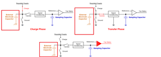
I am working on a touch implementation with a driven shield. It is detailed in the related post. I now have my PCBAs and am seeing some non ideal shield performance.
I am using the OPA357AIDBVR that shares a 3.3V supply with the MSP430.
What I am seeing is:
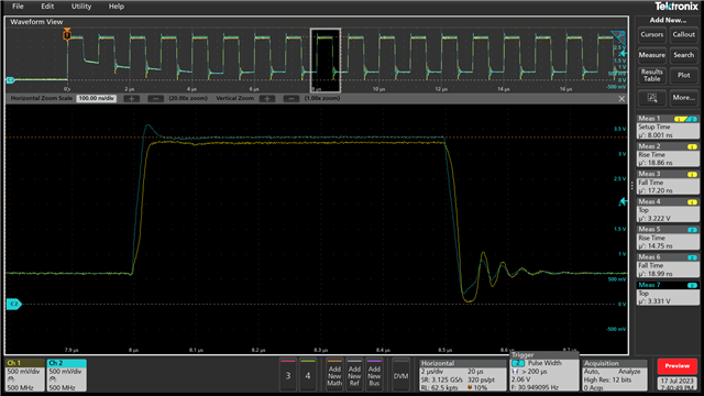
1. The shield lags the touch element by 8ns on the rising edge.
2. I am seeing the touch element overshoot the 3.3V rail.
3. The OPA357 output is 0.111V below my rail voltage despite being a RIRO CMOS device.
4. On the falling edge there is significant ringing, and again some lag. However, there appears to be more drive strength in the falling edge vs rising as to be expected.
Main question is if this matches other implementations that you have seen?
Secondary questions:
1. Should I move the OPA357 to a 5V rail to achieve a 1:1 voltage at the top of the waveform, or is a 0.11V delta acceptable?
2. Is the ringing on the bottom edge caused by the shield capacitively coupling to the touch element and driving it below what appears to be a diode reference? What is this low voltage reference and is noise at this stage problematic to the measurement?
3. Are the rise times and setup delays what you would expect?
I do not have a reference design in front of me to measure for comparison.
Best,
Adam