This thread has been locked.

If you have a related question, please click the "Ask a related question" button in the top right corner. The newly created question will be automatically linked to this question.

UCC28513: The PFC function is lost above 220Vac

Genius 15029 points
Part Number: UCC28513
Other Parts Discussed in Thread: UC3854, UC1854

Hi Experts,

Good day. Seeking your assistance on this query from a customer:

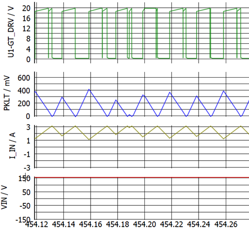
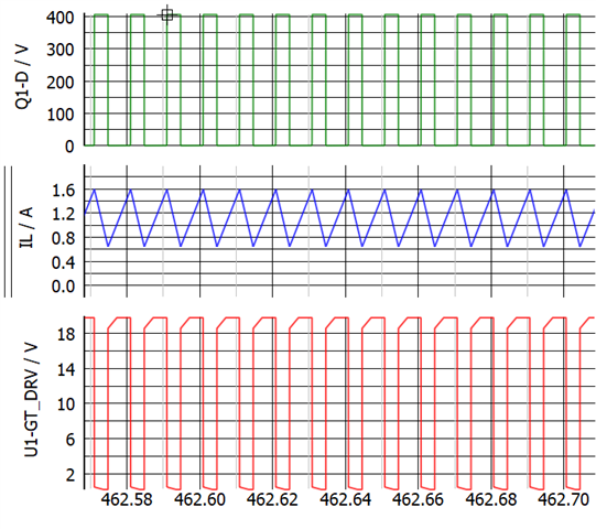
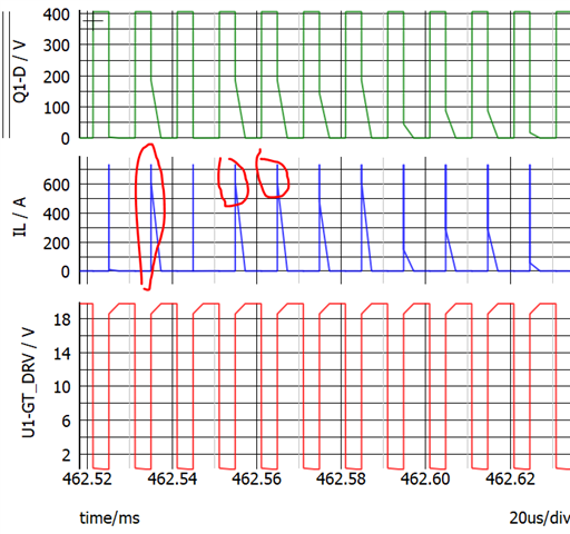
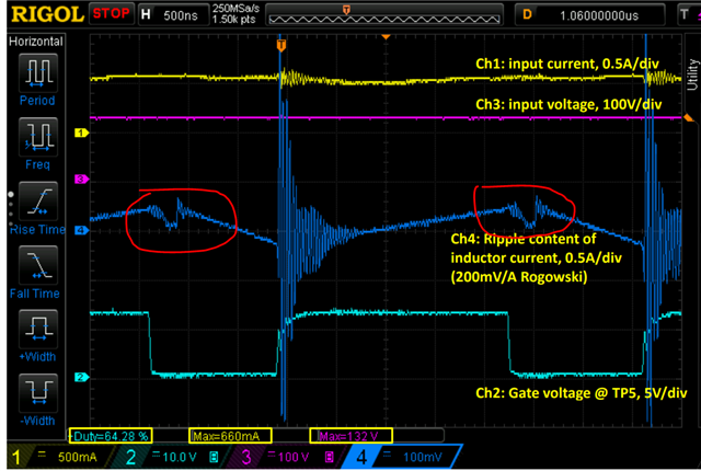
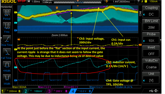
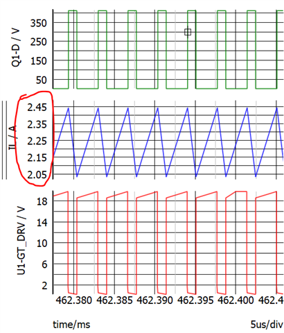
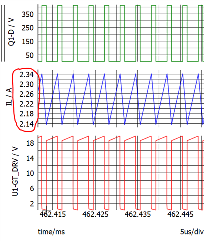
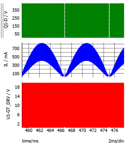
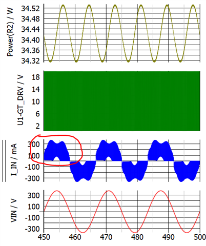
"I have a PFC boost converter design based on the data sheet of this chip. It is a 150W power supply with universal input of 85Vac-264Vac.
The PFC function is lost above 220Vac; I am trying to identify what may cause that.
Not damaged but my duty cycle becomes so small at the peaks of input voltage that i get significant distortions in the current waveform."

Customer have done fair amount of investigation on the problem and wanted to give a complete description of the design, problem encountered, and steps taken to mitigate it.

I have attached the files shared/summarized by the customer about the two queries.

Looking forward to hearing your support. Thank you.

Regards,
Archie A.

QuestionsToPostOn_TIwebsite_11202022.pdf

  • Hi Archie,

    Thank you for the query on UCC28513 and sending detailed report.

    The following would be mu suggestions for the questions in the attached presentation:

    1.  The waveforms at 85V input voltage look good. As we increase the input voltage and come close to 220V, the duty cycle of the becomes very small and this increases the peak currents. In this process the controller enters the DCM mode. The CCM controllers are ideally designed for a peak inductor current ripple ratio of 0.2-0.35. So in DCM mode, the inductor and switched node capacitance start to ring which will potentially lead to instability in current loop and thereby degrade your input current waveform. I checked your report and it says the input current is distorted at 220V at all loads. I would suggest the following, to increase the boost inductor from the current value of 660uH to 1mH or higher so that your inductor current ripple ratio is reduced to less than 0.4 and share your observations. Please share your observations at 220V for different loads.

    2. Regarding question 2, the capacitance mentioned in figure 36 is the maximum allowable capacitance on the ISENSE2 pin, which determines the minimum controllable minimum controllable pulse width on gate 2 output.

    Please let us know if you have any questions.

    Regards,

    Harish

  • Hello Harish,

    Good day and thanks for detailed notes you shared.

    Apology for the delayed update as our customer engaged to some works and just provided inputs:

    Attached file summarizes the results we obtained per your recommendations. The updated results start on page 20.
    Another thing, they have a video file shared, and would like to share it with you (see below). It shows how the PFC is lost and recovered as the supply voltage is increased and reduced.

    Thank you for your continued support.

    Regards,
    Archie A.

    QuestionsToPostOn_TIwebsite_11272022.pdf

    Movie: IMG_4533.zip

    Click here to play this video

  • Hi Archie,

    Thank you for sending the video & files. I understand there is clear flattening of input current waveform and the suggested value of inductor does not work. I will check the loop compensation values for current and voltage loop  and get back to you by tomorrow.

    Regards,

    Harish

  • Hello Harish,

    Thanks for your support.

    We are looking forward to your confirmation with loop compensation.

    Regards,
    Archie A.

  • Hi Archie,

    Please find the attached document containing calculation for the customer specifications.

    I see some discrepancies in the choice  of current sense resistor. I get 0.42 ohms as against 0.22 ohm being used 

    Most of the loop values seem reasonable, although there are some minor deviations. I have included them in the pdf document itself. Please share it with the customer and let me know their comments.

    Thank you

    Regards,

    Harish

    MATHCAD_calculations.pdf

  • Hello Harish,

    Thanks for the guidance and sharing the PDF, customer will try this and give us update.

    Customer has the mathcad tool and asked if it's possible to share to them the original mathcad file? This way they can do some minor adjustment if needed.

    Thank you.

    73,
    Archie A.

  • Hi Archie,

    Please find the attached MATHCAD file for the calculations which I shared.

    Thank you

    Regards,

    HarishUntitled.mcdx

  • Hello Haring,

    Thanks for sharing.

    I have made the changes recommended but the results are not any better. Slides 25-30 show the changes made and the results obtained. It would be nice to get the confirmation that I didn't misunderstand the recommendations.
    Also, I could not open the Mathcad file, the one I have is version 14. If there is any way to save the file in older version, that would be great.

    73,
    Archie A.

  • Hi,

    You might need MATHCAD prime to open this. My version is 8.0

    Can you please share the slides where you made changes?

    Regards,

    Harish

  • Hello Harish,

    Refer to the attached slides:

    QuestionsToPostOn_TIwebsite_12112022.pdf

    For your further assistance.

    73,
    Archie A.

  • Hi Archie,

    Can you please share the inductor current waveform along with gate pulses at both 85/230Vac?

    Thank you

    Regards,

    Harish

  • Hello Harish.

    Happy Monday.

    The latest measurement results start on page 31 of the attached file.

    Regards,
    Archie A.

    QuestionsToPostOn_TIwebsite_12182022.pdf

  • Hello Archie, 

    Harish is out-of-office for a few days.  I will try to help you until he returns.

    Thank you for the additional waveforms.  On slides 36 and 37, I see huge current ringing at the turn-on edge of the MOSFET.  I've seen this before and it is due to significant inter-winding capacitance distributed through the boost inductor.  This high Cw usually comes from using a small diameter core and filling it with multiple layers of turns to make up the inductance.  The multiple layers contribute to the high Cw.  I estimate this ringing at ~20MHz.
    I think the peak ringing might be tripping the PKLMT threshold at Vac > 200Vrms and causing much of the distortion seen above 200Vac.  

    To de-sensitize PKLMT, I suggest to add 100pF across your R5 (R7 in DS).  
    In addition to potential PKLMT triggering, this ringing will also contribute significantly to the conducted- and possibly radiated-EMI signatures. 
    I recommend to change the inductor design to avoid high Cw.  One way is to use a "bank-winding" method of winding, so that the overlap of turns is minimized.  Another way is to increase the core size so that much fewer turns are needed and a single-layer winding can be used.  (Keep a gap between the first turn and the last turn.)   A third alternative is a combination of the two:  somewhat larger core for somewhat fewer turns, and turns done with bank-winding method. 

    Although not shown, I presume there is a "Cin" immediately after the diode bridge.  If not, there should be.  For 120W load, 0.1uF is more than enough, maybe only 0.047uF is needed.  Usually an X-cap is used.  

    In Harish's Mathcad, he targets the current-loop cross-over frequency (fci) to be Fsw/10, and achieves ~36kHz.  Although the switching frequency allows it, I think this bandwidth may be too high for smooth operation.  I suggest reducing the fci to ~10kHz or so, to avoid reacting too fast to small perturbations.  
    Unless I'm mistaken, a quick approximation is to increase C6 and C7 each by 3.6x and decrease R13 by 1/3.6.  

    Please try these suggestions, and let us know what happens. 

    Regards,
    Urich

  • Hi Urich/Harish,

    Thank you for your continued support.

    Customer is following this post and would like to share the new attached file:

    Starting from p37, summarized the test results based on the last feedback you shared.

    For your further assistance. Thank you and Happy Holidays!

    73,
    Archie A.

  • Happy New Year! One of our experts will be back in office after the holidays and answer your questions. Thank you! 

  • Hi Archie

    Thank you for the reply.

    I think from your calculations, with R7 and R14 equal to 1.5k and 10kohm with a sense resistor equal to 0.4 ohms, the peak current limit is set to 2.27A as per the equation below.

    I understand that your changes wrt to slowing down the current loop and playing with the capacitor after diode bridge did not offer much help, but it seems there is definitely PKLIMIT triggering as Uli suggested (with currents going up to 3.4A). So I would also recommend trying to ensure minimizing the switch node capacitance (interwinding capacitance) from the inductor and let us know your observations.

    Regards,

    Harish

  • Hello Harish,

    Thank you. The customer updated with the latest result starts from p58:

    QuestionsToPostOn_TIwebsite_12282022.pdf

    Happy New Year.

    Regards,
    Archie A.

  • Hello Archie, 

    Reviewing the latest response from your customer, I realized that one of my recommendations on Dec 19th was in error. 
    I recommended to put a 100pF cap across R5 to desensitize PKLMT.  That was an error, since it would make PKLMT even more sensitive to noise. 

    What I meant to recommend was to put a 100pF cap from PKLMT to GND (pin 6 of IC), to filter high frequency noise.   
    I still recommend to do that.  

    I also still recommend to change the design of the boost inductor to a larger core for single-layer winding or to accommodate a bank-winding (to greatly reduce inter-winding capacitance).  I believe the existing high frequency ringing noise is likely to be the source of a number of problems, including the sometimes reduction in switching frequency (which normally should not be able to happen).

    Regards,
    Ulrich

  • Hello Archie, 

    I should have added comments on the latest testing results: 
    Removal of C46 (by-pass cap around the current sense resistor R43) showed increase in current distortions at lower input voltages. 
    Conversely, increase of C46 value around R43 showed decrease of distortions until higher input voltages. 

    I think this is consistent with C46 by-passing some the high frequency ringing noise to GND so it couldn't affect PFC operation.
    However, at very high input voltages, the ringing gets worse and some noise gets through to start interfering with signals and causing distortions. 
    I suspect that increasing C46 to 200nF would suppress the noise even more, however this is not a solution since heavy filtering of the current sense will also delay response to real peaks from transient conditions. One can lose proper OC protection.  Also, THD can be increased, since the CS signal will be more distorted from the filtering. 

    Again, getting rid of the source of the high-freq ringing is the best approach.  

    Regards,
    Ulrich

  • Hi Ulrich,

    Happy NewYear! Alex, the customer would like to share the notes below on his behalf:

    I performed the latest recommendations from Ulrich and Harish, here are the comments/questions, if you could post them that would be great:

    1) Removed the 100pF cap from R7 (on data sheet) and added 100pF from pin14 to pin11 (from PKLMT to GND), no improvements.

    2) Question: How does the chip react when PKLMT is activated? Does it effectively reduce ON time and is reset at every cycle (cycle by cycle limiting) or something else? Is there any practical way to confirm/verify that the current limit is reducing the ON time? This is because the high current I measure during turn on may not be completely accurate due to difficulty associated with measuring high frequency current.

    Thank you.

    73,
    Archie A.

  • Hi Archie,

    Happy New Year 2023 to you.

    On the PKLIMIT part it will be activated (the reset input of the flipflop) and it will turn off the gate pulse as soon as the current hits the predtermined set limit.

    Shown below are two simulations with and without the peak limit activated.

    No PKLIMIT activated: 

    When PKLIMIT is activated: There is distortion in input waveform when when PKLIMIT is reached (0V) and cycle by cycle mode kind of behaviour is seen.

    The above waveforms are to demonstrate PKLIMIT functionality and these do not replicate the exact ringing behaviour observed during turn on of FET which is observed in your case. So when PKlimit is hit, RSET of flip flop is high and gate pulses turn off for that cycle, so if the currrent transient is fast, it can reduce ON time for that cycle. You can use this measurement technique just to make sure the measurements are accurate. https://www.cui.com/blog/how-to-measure-ripple-and-transient-in-power-supplies

    Regards,

    Harish 

  • Hi Harish,

    Thank you for these inputs.

    Posting here the comments/queries from Cx:

    1) Removed the 100pF cap from R7 (on data sheet) and added 100pF from pin14 to pin11 (from PKLMT to GND), no improvements.

    2) Question: How does the chip react when PKLMT is activated? Does it effectively reduce ON time and is reset at every cycle (cycle by cycle limiting) or something else? Is there any practical way to confirm/verify that the current limit is reducing the ON time? This is because the high current I measure during turn on may not be completely accurate due to difficulty associated with measuring high frequency current.

    3) In order to prove that the interwinding capacitance is causing the problem, and nothing else, is there any major concern with defeating the PKLMT function temporarily, by lifting pin14 (PKLMT) and shorting it to pin11 (GND)?

    (See my private message, a request from customer).

    Thank you.

    73,
    Archie A.

  • Hi Archie,

    Thank you for the reply.

    I have already provided the behaviour with simulation on the behaviour when it hits PKLMT is activated in my response above.

    You can by pass the PKLMT function as suggested, but I am not sure how big is the actual ring in the waveform is without the PKLMT condition.

    I have accepted the request in e2e forum as suggested in case customer wants to share some confidential information.

    Regards,

    Harish

  • Thanks, Harish.

    Alex (customer) did additional tests last weekend. The latest results start on slides 68. Sharing it below.

    QuestionsToPostOn_TIwebsite_01082023.pdf

    Thank you.

    Regards,
    Archie A.

  • Hi Archie,

    Thanks for reply.

    I think at this point it would be better to take a step back and to try Uli's suggestion to reduce ringing at switching instants caused due to the switch node interwinding capacitance of the inductor by re-designing it.

    Please let us know your observations.

    Regards,

    Harish

  • Hello Harish,

    Thanks for waiting. Cx just finished the additional tests by using toroid inductors.

    The test results start on page 76, posting on customer behalf:

    QuestionsToPostOn_TIwebsite_01152023.pdf

    For your assistance.

    Regards,
    Archie A

  • Hi Archie,

    Thank you for posting the latest result. I will check it and get back to you by tomorrow.

    Regards,

    Harish

  • Hi Archie,

    I understand from the waveforms changing the inductor does not seem to improve the situation from before.

    But when I try an approximate simulation model to replicate your behaviour of high current spikes observed at the instant of gate turn on, this behaviour is predominant when there is some capacitance in the order of 80pf or above. The following are the waveforms which show this behaviour.

    Normal behaviour:

    With capacitance effect:

    So, I feel this is still due to capacitance effect coupling.

    Please refer to the following application notes on boost inductor design from Mag-inc. Koool-mu / Sendhurst cores material is preferable.

    https://www.mag-inc.com/Products/Powder-Cores/Kool-Mu-Cores/PFC-Boost-Design

    https://www.mag-inc.com/Design/Design-Guides/Inductor-Cores-Material-and-Shape-Choices#:~:text=Core%20Material%20Properties,iron%2C%20and%20molybdenum%20alloy%20powder.

    Also refer to this app note (pages 16,17) on interwinding capacitance effect.

    an53 (2).pdf

    Measuring interwinding capacitance can be tricky, I would recommend using a bode anlyzer for this as described in the following app notes.

    https://www.omicron-lab.com/fileadmin/assets/Bode_100/ApplicationNotes/Transformer_modelling/App_Note_Transformer_modelling_V_2_0.pdf

    https://www.omicron-lab.com/fileadmin/assets/Bode_100/ApplicationNotes/Impedance_Measurement_methods_using_the_Bode_100/2020-10-21_Bode_Appnote_Impedance_Measurements_V1_0.pdf

    https://www.coilcraft.com/getmedia/8ef1bd18-d092-40e8-a3c8-929bec6adfc9/doc363_measuringsrf.pdf

    Thank you

    Regards,

    Harish

  • Hello Harish,

    Customer seeing this post and he responded:

    "I did see the reply and will go through the references carefully. Thank you so much for your help!
    It may take a while until I get updated results."

    Requesting to keep this link/thread open.

    Thank you.

    Regards,
    Archie A.

  • Hi Archie,

    Sure, we will keep this open. Please let us know their feedback.

    Thank you

    Regards,

    Harish

  • Hello Harish,

    Thank you. Customer has an update:

    I have done additional tests and the latest results start on p82.
    Thank you.
    73,
    Archie A.
  • Hi Archie,

    Thank you for the detailed report. I will analyze this and get back to you tomorrow.

    Regards,

    Harish

  • Hi Archie,

    Can you please provide PPM ID and opportunity details for this project?

    Thank you

    Regards,

    Harish

  • Hi Archie,

    The following are my observations:

    First of all, glad to know that changing inductor with reduced interwinding capacitance helped reduce the turn on spikes. The very fact that your inductor current waveform had a dip as shown in red below shows the presence of strong capacitance and the momentary dip signifies this.

    Second, using an oversized inductor should not contribute to the phenomenon attributed below. The fact that inductor current keeps increasing inspite of DRV turn off seems strange.

    The follwoing screen shots show using 750uH inductor to 1.5mH inductor. It only reduces the current ripple ratio with increased inductor as shown below:

    I ran a few simulations for your system specifications (120W/277khz/85-265Vac/400V) and used UC3854 which is similar to UCC28513 PFC and it has a ready simplis model available.  

    120W/85Vrms/400V                                        30W/85Vrms/400V

    30W/265Vac/400V                                     120W/265V/400V

    So at 30W you expect to see distortion in current waveform, but it should be better than what you had attached. I tried optimizing the loop parameters and have attached the simplis file. Please use this as reference to try to tune your loops which I think it should provide better results. Also attached is the Pdf of the simplis schematic.

    Schematic.sxsch

    8475.Schematic.pdf

    Thank you

    Regards,

    Harish

  • Hello Harish,

    There is a posting on E2E board, it seems very useful. I have following questions to Harish:
    1) What version of Simplis are you using? I have the free version, 8.50i. Do I need the licensed version to run the file?
    2) When I try to run the simulation file in Simplis, I get the error message that it is unable to locate subcircuit UC3854. A quick search on line didnt yield any results about the Simplis model of UC3854.
    Regards,
    Archie A,
  • Hi Archie,

    I use Simplis version 9.0 which is provided by our company.

    You should be able to find the model of UC3854 under Place >> Symbol library >> PSU Controllers >> Vendors >> UC1854

    If this is not available in trial version, then you might need a full version of Simplis. You could try contacting simplis customer support, I have found them to be helpful with these issues.

    Also Archie could you please post future queries related to UC3854 in a separate thread for tracking purpose. The only purpose of introducing UC3854 here was to analyze the current and voltage loop due to unavailability of spice model for UCC28513. I would kindly request you to "click resolved" if the above suggestions were helpful and start a new post for questions related to UC3854.

    Thank you

    Regards,

    Harish

  • Hello Harish,

    Thank you very much for your commendable support.

    Regards,
    Archie A.

  • Thank you Archie,

    Please let us know if you have any questions with a new post.

    Regards,

    Harish