This thread has been locked.

If you have a related question, please click the "Ask a related question" button in the top right corner. The newly created question will be automatically linked to this question.

UCC27511A-Q1: PFC mosfet low side driver IC failure when boosting to 390 V

Part Number: UCC27511A-Q1

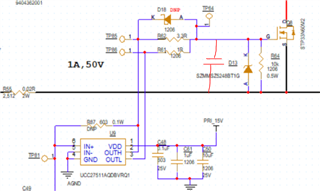
The driver UCC27511AQ was damaged whenever the PFC voltage of 390V builts up (whenever IC comes into action which is above 65V  output )
Mainly PIN 1 (VDD) and PIN 2((out1) tracks were damaging. Is there anything to do with the ground connections? ( because  GND pin of IC is connected to AGND and 15V IC  power supply  is connected to PGND and they both are shorted through a 0 ohm resistor)power_control_merged.pdf

I am  attaching a PDF of the PFC section and auxiliary supply section  for your reference  


  • Hi Hema,

    So the driver starts to fail only when the output voltage is ramped up to 390V? And is it an instant/guaranteed failure or random? There are a few good choices for things that could be causing damage. Firstly, the split between AGND and PGND should ideally not cause any issues. If they are connected via a 0Ω, they should be equal. In reality, those jumpers have some resistance and inductance, but I don't know if the current flowing through that loop would be large enough to cause a significant drop. The A version of this device can handle some negative voltage on the input pins. 

    I think the two most likely answers based on the damage you see, is that the rise to 390V is causing a surge on VDD, or injecting noise into the driver. A measurement of VDD-PGND when the voltage is ramping up could help us determine if the VDD is the problem. Otherwise, a scope capture of the gate waveforms can help us tell if that is the issue. This design looks very similar to TIDA-00779, so we can look at differences from that as possible sources of the problem.

    Thanks,

    Alex M.

  • Thank you for your instant Reply

    It is a random failure, Failure is not occurring every time but 40 percent time it is happening whenever it boosts the voltage

    I am attaching the PCB layout for the PFC section which includes many details

    Please refer to and confirm. Please share every possible solution for the problem we are facing so that we can test and confirm 


    pfc section.pdf

  • Hello Hema,

    The randomness may have to do with the AC input's state when the IC activates. I found in my simulation that the noise (gate voltage ringing) is worst near the AC 0 crossings. 

    Here are some things that may help:

    1. Adding extra Cgs capacitance will reduce ringing, at the cost of increased switching losses.
    2. Increasing Rgs will have a similar effect
    3. Using a ferrite bead instead of/with gate resistors can filter out high frequency ringing
    4. Some series resistance/inductance on VDD (before the bypass capacitance) can filter out any ringing/transients on VDD
    5. Changing the ground connections may help. If you trace the turn-on and turn-off loop of the driver considering the ground connection, it is longer than ideal. This can add inductance to the gate driver loop (a fairly high di/dt net) which can lead to ringing and damage. The fixes suggested in 1-3 may help regardless though. 

    Best of luck with the testing. If you can get any scope captures, it helps a lot to see what the potential problem is, and hopefully reduces the amount of destructive tests that need to be run.

    Thanks,

    Alex M.