This thread has been locked.

If you have a related question, please click the "Ask a related question" button in the top right corner. The newly created question will be automatically linked to this question.

UCC28065: Trigger condition of Overcurrent operation. (180-degree shift Interleave operation change to same phase operation.)

Part Number: UCC28065

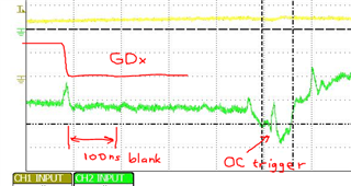
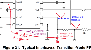
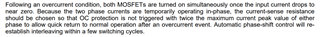
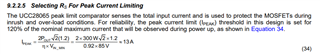
Over current operation of UCC28065. 

When overload operation occurs,
the 2 gate-drive output, which was previously operated 180 degrees out of phase, is turned off at the same time.
(See the operation waveform of the attached file.)
 At this time, operation occurs under conditions different from both Ton-max and the threshold voltage of the CS pin.
Please tell me the operation judgment conditions that cause the trigger for this OC operation to be turned off at the same time.

UCC28065_Overcurrent_operation_20230619.pptx

  • Hello, 

    Thank you for your interest in the UCC28065 Interleaved PFC controller. 

    The reason for OC operation at -146mV on CS is because there is additional noise on the CS signal that exceeds -200mV.  
    With tip& barrel probing on CS and 5us/div sweep rate, you may be able to see it on your oscilloscope. 
    You may need to increase your filtering on the CS input to eliminate the noise. 

    This OC response happens at the peak of the 100-Vac input, where the input currents per phase is highest. In your zoomed screenshot, you can see that the blue and purple gate drives are interleaved until suddenly the blue gate drive turns off when the purple drive goes low.  The turn-off edge of the purple channel adds enough noise to the CS signal that the -200mV threshold is reached.  

    After that moment, both phases stay in phase for some duration  until the input voltage forces the current to be low enough to break the noise condition and resume normal operation.  Note that the 200mV threshold is consistently reached because there is no noise while both phases are conducting.  It is at the turn-off edge of one of the phases that noise from one phase might interfere with operation of the other phase. 

    I suggest to try doubling the R-C time constant of the filter on the CS pin.  IF that doe snot improve things, there may be a layout problem where noise couples around the filter. 
    Mitigation of a layout problem will take more effort. 

    Regards,
    Ulrich

  • Dear Ulrich

    Thank you for your reply.

    I retransmit the magnified waveform. Please refer to the attached file.
    Attached pptx file 1st page:
    On the IC block diagram, the CS function provides 100ns blanking.
    Noise exceeding the 100ns threshold voltage cannot be observed on the waveform.
    (In the oscilloscope measurements, the settings are set so that they are not affected by switching noise as much as possible, but they cannot be completely eliminated.)
    2nd page, 
    According to your advice "With tip& barrel probing on CS and 5us/div sweep rate, you may be able to see it on your oscilloscope. "
    I took waveform with 5us/div.
    It seems different that the noise you described is above the threshold.
    It is difficult to understand this behavior just by what is described in the catalog.
    If possible, I would like to get the answer from the engineer (or section member) who is developing this IC to inquire about the control specifications of the IC.
    Best regards.

    UCC28065_Overcurrent_operation_Magnified_waveform_20230621.pptx

  • Hello, 

    Thank you for the updated measurements.  
    I see there is a lot of ringing on the CS pin waveforms (green traces). None of this ringing appears in the actual PFC current shown in Channel 1 (yellow traces).  Do you have an R-C filter to GND on the CS pin? 
    There should not be so much ringing if there is an RC and if the capacitor has minimum path lengths to CS and AGND. 
    Typical values are 100ohm and 10nF. 

    So much ringing suggests that either there is insufficient filtering on CS or the filter capacitor is terminated to a GND point far from the AGND pin (pin 6) of the UCC28065 and the GND path has oscillating current in it.  

    Here is a website that describes two types of tip & barrel probing:  https://www.electronicspecifier.com/products/power/oscilloscope-probing-techniques-for-measuring-power-supply-ripple 
    I have used both methods, and the "paperclip" method works well when you have to probe over the top of an IC.  The UCC28065 responds to the signals that it "sees" at its pins with respect to AGND.  If your oscilloscope GND point was away from pin 6, there may be "ground-bounce" from ringing di/dt through stray inductance that is superimposed on the current sense signal. 

    On slide 2 of your file, you show some peak noise exceeding -200mV that is less than 100ns in duration. 
    However the 100-ns blanking time is applied on the rising and falling edges of the gate drives. 

    Please check the waveforms of GDA and GDB with respect to Vcs.  I think that the gate drive has fallen about 400ns before the peak CS voltage and the 100-ns blanking had already expired.  If your MOSFET is large or has a high gate resistance, it may have a 400-ns turn-off delay. 

    If this is the case, I suggest to try increasing the value of the CS filter cap (if there is one).  
    But most importantly, the filter cap for CS should connect to CS and AGND as close as possible to the IC pins, as seen in the PCB layout example of Figure 36 on page 47 of the datasheet.  Keep high power currents out of the AGND net.  

    Regards,
    Ulrich

  • Dear Ulrich

    Thank you for your reply.
    I understand.100ns blanking is gate drive edge blanking. 

    Since interleaved PFCs use high power, FETs with higher current ratings are used. (The main purpose is to reduce Ron and reduce heat generation.) Since FETs with high current ratings have high gate capacitance and are used to reduce switching speed due to EMC measures, FET switch will be delay over 100ns easily, so I did not think 100ns blanking is from the drive edge.

     CS terminal already 100ohm and 10nF CR filter is provided. (The capacitance increasing are no effect for this issue.)

    I intended to explain that common mode noise is superimposed on the oscillo measurement waveform by showing the measurement waveform of GND in the previous document, but it was not understood, so this time I will add the differential waveform of the CS pin and GND and retransmit it.

    Please refer to the attached file 1st page.  (UCC28065_Overcurrent_operation_differential_waveform_20230623.pptx )

    Please refer to page 3 of the same attached file for the reason why I thought the trigger for OC operation is not the threshold of -200mV for the CS pin.
    I hope that you will be able to correctly understand the questions about the phenomenon I am proposing.

    Best Regards

    UCC28065_Overcurrent_operation_differential_waveform_20230623.pptx

  • Dear Sir, 

    Thank you for the additional waveforms and diagrams.  Let me assure you that I did understand the phenomenon that you proposed about common mode noise superimposed on the signal.  In fact I was trying to convey the exact same message to you, except I think it is more than noise pick-up on the 'scope probe.  Instead, I think it is real GND noise from MOSFET turn-off coupled to one side of the CS filter cap which carries the noise into the CS pin. 

    Please see my sketch of this.   

    The controller acts on the signals that it sees at its input pins with respect to its AGND pin, not to GNDs anywhere else in the system.   

    If the filter cap GND is not close to the AGND pin, and if switching currents travel through the path between the cap GND and the AGND pin, then stray inductance in that path will generate noise which superimposes onto the voltage waveform from the current sense resistor. 
    In this case, increasing the cap value will not solve the problem.  Only diverting the switching current to another path will solve it. 
    That is why I mentioned the PCB layout example in Figure 36, so that you can examine your design to compare.   

    I completely understand and agree with your diagrams on sheet 3.  
    If your sense resistor value is not low enough to accommodate two maximum peak inductor currents in-phase, then it will result in reduced average current as shown at the bottom of slide 3.  The UCC28065 datasheet describes this on page 32, and the peak current equation (34) to design Rs (eqn 35) takes this into account on page 41.  

    If the CS cap GND path cannot be improved, perhaps the only solution left is to reduce the value of Rs.

    Regards,
    Ulrich

  • Dear Ulrich
    Thank you for your patient support.
    I have confirmed that the AGND you presented is the cause of the problem.
    The phenomenon was improved by connecting the filter capacitors between the CS pins and AGND pin directory with the shortest conductive wire.

    Please refer to the attached file waveform.

    After Improved Waveform at UCC28065_Overcurrent_operation.pptx
    In my pattern design, I try to be possible using TI Ics and other companies' ICs together as alternative parts.
    However, it is difficult to improve the AGND because the AGND pin is changed to a functional pin at other companies' Ics (not AGND).
    In the next pattern design, I would like to introduce an ideal AGND connection on a dedicated pattern for TI ICs.

    Best Regards