Other Parts Discussed in Thread: TUSB1064, , TUSB1002, TUSB1002A
Hello,
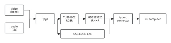
We used TUSB1002RGER and HD3SS3220IRNHR. When the speed is 5Gbps, both sides of usb work normally. When the speed is 10Gbps, only one side of usb works normally.
The circuit schematic is attached. Could you please help check whether there is any circuit problem?
We also tried TUSB1002RGER and VL160, and both usb sides worked well at 5Gbps and 10Gbps speeds; The project is used to transfer the collected information to the computer through usb, and the application is UFP;
Posts with similar issues : HD3SS3220: HD3SS3220: Only one side of the usb-c is working, design review/debugging - Power management forum - Power management - TI E2E support forums;
->The post discusses yes DFP, I'm not sure if it applies to UFP, for example:
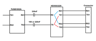
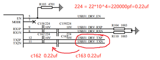
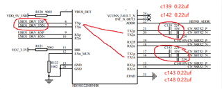
1. Is coupling capacitance required between TUSB1002RGER and HD3SS3220IRNHR? Or direct DC coupling?
2. Do the RX1 and RX2 of the HD3SS3220IRNHR require coupling capacitors?
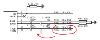
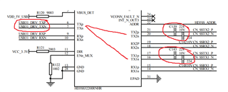
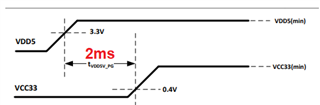
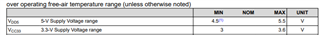
3. Do I need to ensure that the VDD5 pin voltage remains stable for 2 ms before the VCC33 pin rises? VCC33 We use slow rise instead of delayed rise. Is slow rise feasible?
4. The VBUS_DET pin of HD3SS3220IRNHR is connected with 5V voltage, do I need to control the timing of VBUS? It is now out of control.
5. We did not use 3.3V voltage, but 3.0V. Does this have an impact?