A related question is a question created from another question. When the related question is created, it will be automatically linked to the original question.
If you have a related question, please click the "Ask a related question" button in the top right corner. The newly created question will be automatically linked to this question.
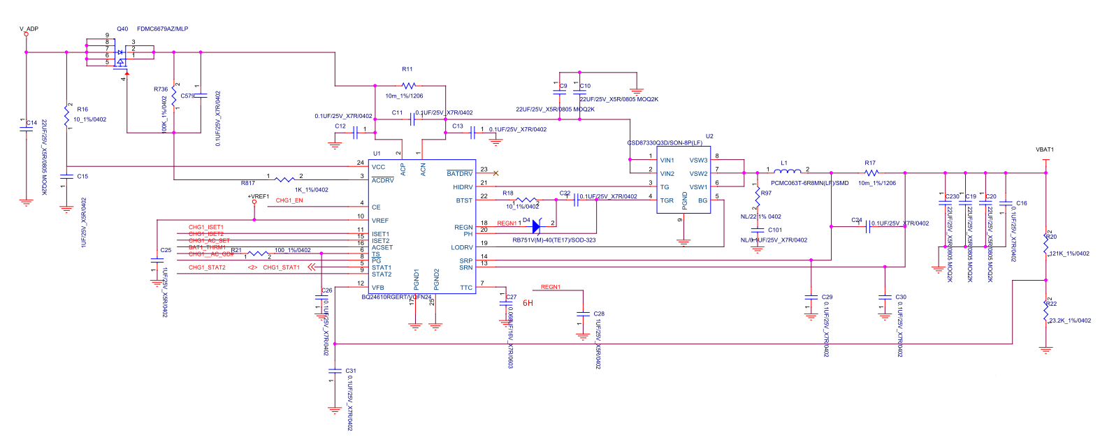
BQ24610: Boost from VBAT damage MOSFET and BQ24610
Please use fresh units and show scope capture at the battery insertion. Probe at VBAT1, VSW .
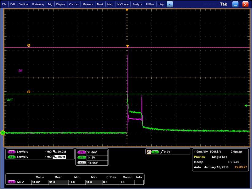
When adapter is not present, plugging in VBAT should bq24610 should not switch. Therefore, it is very unlikely to have 29V at SW node with 12V battery hotplug in.
Sorry click on the bottom by mistake.
Looking at your schematic, a 22uF cap needs to be added at the VBAT1 node close to the battery. However, this should not cause the voltage spike. We have customer using this part for 5cells and 6 cells for a long time but have not had hot plug in damage on our part.. Please submit the IC for FA so we can get information on which pin is been damaged on the bq24610.
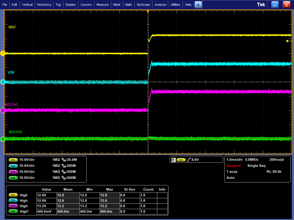
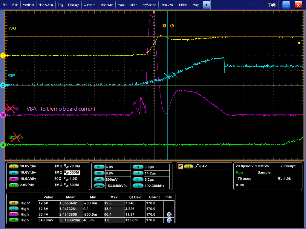
We are try to remove BQ24610EVM Q5, but we are see the VSW have boost 18V voltage & current probe measure 66,4A.
if we add Q5 same condition on customer PCB, then boost issue solve Rise is Smooth.
if this application only 5~6 charger docking board not have system side on PCB, then Q5 is must? or change to Schottky or diode? or any suggest share for me?
Thank you very much.
if customer want to use the shottcky diode,
then we need to concern about Forward Current or Forward Surge Current? how many current value is Safety?