This thread has been locked.

If you have a related question, please click the "Ask a related question" button in the top right corner. The newly created question will be automatically linked to this question.

BQ76940: BQ76940 Schematic Review

Part Number: BQ76940
Other Parts Discussed in Thread: TIDA-010030

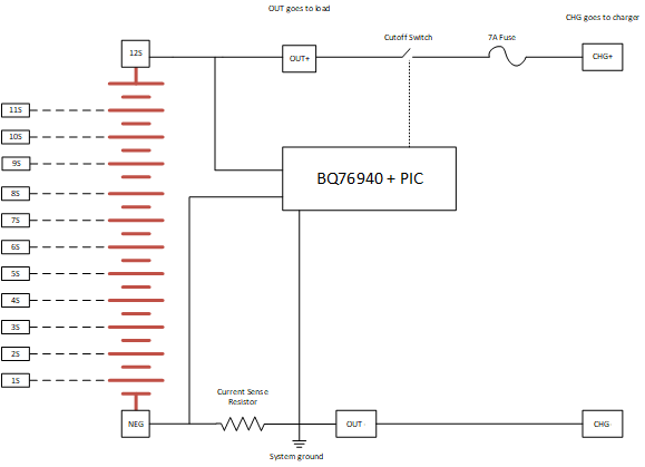
I have finished my BQ76940 schematic (attached).  I'm attaching a block diagram that may help show what I'm trying to do.  I followed the Top 10 Design Considerations, TIDA-010030, and the schematic video.

I decided to use the current sense circuit.  I've connected the current sense pins in a way that makes sense to me.  Can you check if I have it connected OK?  I think in the top 10 design considerations doc it allows what I'm trying to do, but do I need shotkeys on either side of the current sense resistor for protection?

Also, since I'm not using CHG/DSG pins, do I really need to make use of the ALERT pin?  I have a dedicated micro, can I just poll the status registers?

I'm using external N-channel balancing, 20mA.  I put a TVS diode across each cell because the battery connections will be made with a welder.  I've simulated the balance circuit in LTspice and it works well.  I found the MOSFET Vgs_th(max) needs to be low...

And finally, can you check the voltage ratings on the caps I have selected?

Any other suggestions before I start layout?  I think I still need to add a TVS at the top of the pack and at the charger input.

Thanks!

Erik

 BMS12S.pdf

  • Hi Erik,

    I responded to this yesterday on this post,  https://e2e.ti.com/support/power-management/f/196/t/866241  but it is not there today and the system did not seem to save the response, so:

    The schematic displays cut off on the right and bottom and with the component information missing or misaligned.  As an example the link at C11 is for a thermistor.

    • The balance circuit looks ok, but its connection on page 14 has problems for some cells.  Example: U_balance_cell_12 CELL_GATE should connect to the right side of R11 rather than R10.  U_balance_cell_9 looks connected properly
    • With the right side of the connections to BQ76940 missing it can't be checked, but you seem to have taps for the clamp diodes and power for the IC with points A & B identified. See the general figure 15 in the data sheet and details in the application notes/video.
    • Your input filter caps Cc, C7, C9, etc show 1 uF like the EVM, this value can have voltage errors during balancing due to filter settling time.  You might use 0.22 or 0.1 uF if suitable.
    • The 1uF Cc caps are 6.3V if the random link is correct.  If you balance every other cell the voltage on the unbalanced cell between will double, so 8.4V in many applications, check yours.  Select a cap according to your organization's derating guidelines, often this might be 10, 16, or 25V.
    • You don't need to use ALERT if you don't want it, but keep the pull down recommended and avoid noise coupling onto the pin.  Also your software should clear the status when found high to minimize the effect of the dIALERT current shown in the data sheet.
    • For the group power supply caps, each group will have about 4.2V/cell x 4 cells or 16.8V.  Again with derating you might pick 25, 35 or 50V components. 
    • For the output capacitors CAPn, REGOUT, normal voltage is 3.3V, a 6.3V component may be suitable.
    • Grounding the sense resistor at the battery side allows a typically larger discharge current to move the SRN pin voltage positive which has a much higher abs max range in the positive direction than negative.  This does modulate the voltage of signals referenced to "OUT" by the load current acting on the sense resistor and path impedance.  The normal recommended connection is to reference or ground at the battery side.  Note the recommended range of SRP is +/- 10 mV.  With the connection on the "OUT" side, the SRP will go negative with load current.  You can protect the pin with a Schottky diode at the pin, but this is not the recommended range, and remember that a diode is not ideal and has a V-I curve which will vary with temperature.   It could introduce a non-linearity into your currrent measurement.

    For layout:

    • For signals referenced to the BQ76940 VSS, be sure to filter at the VSS potential, connection like the data sheet figure 19 vs 20.
    • Use Kelvin connections at the sense resistor, route differentially to the filter components.
    • Use general electronics routing guidelines, signals should reach the filter capacitor before the IC pins.
    • Be aware that the TIDA illustrates a operational example, but may not be suitable for all systems.  If you have a high field requirement you may need to add circuitry to attenuate signals picked up in the cell interconnect where it enters the board.  Use techniques common to your industry.

  • Sorry for the schematic error and confusion.  I've corrected my mistakes and updated the schematic based on your feedback.  I'm using X7R everywhere so I don't think I should need to derate much.  Thanks for the help!

    7713.BMS12S.pdf

  • Hi Erik,

    C23, C25, C26 look like filter resistors for the SRP & SRN, they would connect at the top of the 100 ohm R26 & R27 to match the data sheet & EVM schematic recommendations.

    All I see.  Hope this helps.