This thread has been locked.

If you have a related question, please click the "Ask a related question" button in the top right corner. The newly created question will be automatically linked to this question.

UCC28950: TI E2E 28951 Transformer input waveforms distorted by applying load

Part Number: UCC28950
Other Parts Discussed in Thread: UCC27324

SIRS,

I AM IN NEED OF YOUR EXPERT WAVEFORM DIAGNOSTIC SKILLS. THE PROJECT I AM WORKING ON USES THE UCC28950 IC.ALL MY OUTPUT SIGNALS, IN MY OPINION, LOOK ABOVE AVERAGE. HERE IS A QUICKVIEW OF MAJOR COMPONENTS USED:

PSFB IC: UCC280950   (fsw:100KHz)

GATE DRIVE TRANSFORMER: COILCRAFT SD250-3L (double-ended)

DC LINK VOLTAGE: 400VDC <2% ripple

MOSFET: IPW60R170CFD7XKS (650V, IDpulse 51A)

Power Transformer: Ratio 12:1, Lmag: 1mH, Llk: 14.22uH

Gate Voltage: 8.5VDC

Watts (max): 1,250 watts

LS not used -- LS -13.32uH - Calculated Ls is Negative and Ls Might Not be Needed

Now, the problem, which I see as a problem.

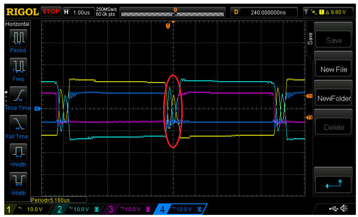
**PIC#1 : Q2 DRAIN WAVEFORM no load. GOOD DRAIN SIGNAL.


**PIC#2 : YELLOW, Q1 Q2 ACTIVE LEG, no Transformer Secondary load

                   TEAL, Q3 Q4 PASSIVE LEG, no Transformer Secondary load

                                GREAT SIGNAL, NO LOAD YET.


                   WORRIED ABOUT THE AMOUNT OF DELAY TIME

**PIC#3 : PT1 TRANS INPUT (YEL out AB fall, teal out CD rise) @100ns no load

                                ZOOMED IN TO 100ns FOR BETTER LOOK

                                I AM NOT SURE THIS IS A GOOD DELAY

                   WORRIED ABOUT THE AMOUNT OF DELAY TIME


PIC#4 -- PT1 TRANS INPUT (YEL out AB rise, teal out CD fall) @100ns no load

                   ZOOMED IN TO 100ns FOR BETTER LOOK

                                I AM NOT SURE THIS IS A GOOD DELAY

                   REALLY WORRIED ABOUT THE AMOUNT OF DELAY TIME


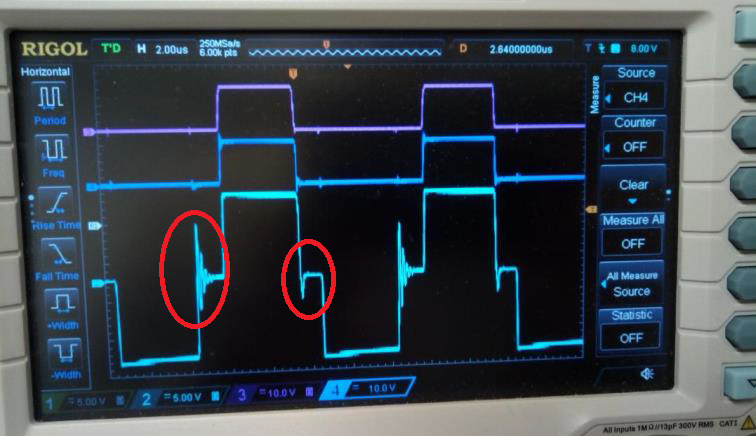
PIC#6, #7, #8 -- Now a load has been applied to the transformer secondary output winding. PIC#6 with 1.2 A resistive Load, PIC#7 with 2.4A resistive Load and PIC#8 with 3.6A resistive Load.

Notice how the waveform changes only when the load is applied. Notice also that the waveform only changes on the passive leg at positive rail and the active at negative rail. Notice that as load is increased, the waveform appears to be dividing. I say dividing because the last current test, which I was not able to record, DID DIVIDE. It actually divided into two complete side by side signals. I immediately shut the system down therefore, that is why I did not get a waveform pic.


QUESTION 1: AS EXPLAINED ABOVE REGARDING PIC#6, #7and #8, I AM LOST. I HAVE EXHAUSTED YOUR FORUM REGARDING THESE SIGNALS. PLEASE DIAGNOSE THE PROBLEM WITH THE WAVEFORMS AND LET ME KNOW YOUR IDEAS AND SUGGESTIONS.


QUESTION 2: PIC#3 and PIC#4 REGARDING THE DELAY TIME. PLEASE REVIEW THE WAVEFORMS AND LET ME KNOW ANY CONCERNS/SUGGESTIONS.


EDDIE LOY

see attached waveforms in the link below:

/cfs-file/__key/communityserver-discussions-components-files/196/TI-E2E-28951-Transformer-input-waveforms-16mar20---1236.pdf

  • Hello Eddie

    Thanks for the clear waveforms. It looks to me like there is something wrong in the signal path from the OUTx pins to the MOSFET gate - this is what I would check first.

    Can you check the OUTA, OUTB signals at the pins of the controller and also at the gates of the MOSFET switches.

    Can you also check the OUTC, OUTD signals at the pins of the controller and also at the gates of the MOSFET switches.

    Please look  at the OUTA/OUTB and the OUTC/OUTD delays at the IC. The waveforms at the gates of the MOSFETs should follow the OUTx signal driving them, please check this.

    You should also check that the SR gate drive waveforms are following the OUTE/OUTF signals.

    BTW: Tomorrow, 17th March is a public holiday in Ireland. I won't be able to reply until 18th.

    Regards

    Colin

  • Thank you Colin.  I will get back to you tomorrow or the following day.

    EDDIE LOY

  • COLIN,

    CORE PROBLEM:

    I AM STILL DESTROYING MOSFETS BY THE DOZEN. I HAVE RUN THE SYSTEM WITH MOSFETS, TRANSFORMER, AND RESISTIVE LOAD OF 8ADC FOR 20 MIN.  THEN BOOM,  EITHER 2 OR ALL FOUR MOSFET ARE DESTROYED. THEN THERE ARE TIMES WHEN THE SYSTEM ONLY RAN ONE MINUTE.  I HAVE WENT THRU 14 MOSFETS IN THE LAST FOUR DAYS.  Q3 & Q4 AND YES I AM ORDERING ANOTHER 14 MOSFETS.  AS YU CAN SEE, I NEED HELP WITH THE CORE PROBLEM

    I WANT YOU SEE WHAT IS ON THE SCOPE SCREEN IN A ORDERLY SEQUENTIAL FASHION IN HOPE THAT YOU WILL SEE THE ERROR THAT I KEEP MISSING,THUS DESTROYING MOSFETS.

    CHECK OUT ATTACHMENT 3, THIS IS WHERE I BELIEVE THE PROBLEM IS AT.

    NO HV RAIL, NO MOSFETS USED IN THE FOLLOWING ATTACHMENTS.

    ATTACHMENT #1  UCC28950 PIN22 OUTA--PIN21 OUTB SIGNAL

    /cfs-file/__key/communityserver-components-multipleuploadfilemanager/bb3de690_2D00_be36_2D00_4e3b_2D00_89f2_2D00_c6eeed3add19-78544-complete/WORD-UCC28950-24MAR20-2350-PIN22-OUTA-_2D00_-PIN21-OUTB-SIGNALS.docx

    ATTACHMENT #2  UCC28950 PIN22 OUTA--PIN21 OUTB SIGNAL 

    /cfs-file/__key/communityserver-components-multipleuploadfilemanager/bb3de690_2D00_be36_2D00_4e3b_2D00_89f2_2D00_c6eeed3add19-78544-complete/WORD-24MAR20-2350-PIN20-OUTC-_2D00_PIN19-OUTD-SIGNALS.docx

    ATTACHMENT #3  UCC28950 GDT SEC#1 - Q1, GDT SEC#2 Q2 (NO MOSFETS)

    /cfs-file/__key/communityserver-components-multipleuploadfilemanager/bb3de690_2D00_be36_2D00_4e3b_2D00_89f2_2D00_c6eeed3add19-78544-complete/UCC28950-OUTC_2D00_OUTD--_2D002D00_--GDT-OUTPUT-Q3_2D00_Q4-WITH-NO-MOSFETS--23MAR20--0700.pdf

  • THE LINKS DO NOT WORK.  I AM RESENDING

  • THE LINKS DO NOT WORK.  I AM RESENDING

    COLIN,

    CORE PROBLEM:

    I AM STILL DESTROYING MOSFETS BY THE DOZEN. I HAVE RUN THE SYSTEM WITH MOSFETS, TRANSFORMER, AND RESISTIVE LOAD OF 8ADC FOR 20 MIN.  THEN BOOM,  EITHER 2 OR ALL FOUR MOSFET ARE DESTROYED. THEN THERE ARE TIMES WHEN THE SYSTEM ONLY RAN ONE MINUTE.  I HAVE WENT THRU 14 MOSFETS IN THE LAST FOUR DAYS.  Q3 & Q4 AND YES I AM ORDERING ANOTHER 14 MOSFETS.  AS YU CAN SEE, I NEED HELP WITH THE CORE PROBLEM

    I WANT YOU SEE WHAT IS ON THE SCOPE SCREEN IN A ORDERLY SEQUENTIAL FASHION IN HOPE THAT YOU WILL SEE THE ERROR THAT I KEEP MISSING,THUS DESTROYING MOSFETS.

    CHECK OUT ATTACHMENT 3, THIS IS WHERE I BELIEVE THE PROBLEM IS AT.

    NO HV RAIL, NO MOSFETS USED IN THE FOLLOWING ATTACHMENTS.

    ATTACHMENT #1  UCC28950 PIN22 OUTA--PIN21 OUTB SIGNAL

    WORD UCC28950 24MAR20 2350 PIN22 OUTA - PIN21 OUTB SIGNALS.pdf

    ATTACHMENT #2  UCC28950 PIN20 OUTC--PIN19 OUTD SIGNAL 

    WORD 24MAR20 2350 PIN20 OUTC -PIN19 OUTD SIGNALS.pdf

    ATTACHMENT #3  UCC28950 GDT SEC#1 - Q3, GDT SEC#2 Q4 (NO MOSFETS)  (Q1 Q2 WAVEFORMS LOOK IDENTICAL)

    UCC28950 OUTC-OUTD -- GDT OUTPUT Q3-Q4 WITH NO MOSFETS 23MAR20 0700.pdf

  • Hello Eddie

    I think that the problem may be that the gate drive voltage is only 8.5V. The Infineon data sheet would seem to suggest that the device can carry 4A with 8V of gate drive but to be honest I'd prefer to drive the gates harder, 12V is fairly normal and the Coilcraft GDT you are using has a 1:1:1 ratio so you should be getting 12V at the gate.

    1/ Use the setup you used for Attachment #3 and measure the voltage on the primary and secondary of the GDT. If the primary is being driven with 12V then the secondary should be at 12V also. If the turns ratio is not 1:1:1 then check with Coilcraft (and perhaps double check the part number on the GDT!)

    2/ What gate drive IC are you using - the OUTx signals from the UCC28950 are not strong enough to drive a GDT directly so a gate driver IC like the UCC27324 is needed to drive the GDT primary.

    3/ What VDD rail are you using for the Gate Driver IC ? and are the Gate Driver IC outputs going from 0V to VDD ?

    4/ The signal outputs at OUTA and OUTB look good. There is a 500ns dead time which may not be optimum but for now it should be ok. The signal rise and fall times look reasonable too.

    5/ The signal outputs at OUTC and OUTD look good. The 800ns dead time may be a bit too long - it just depends on the nature of the power stage you are driving. The OUTC to OUTD delay time is normally less than the OUTA to OUTB delay time because there is more energy available to drive the AP (QC/QD) transition than the PA (QA/QB).

    6/ The ringing during the 'dead time' is due to some resonances between stray capacitances (winding capacitance) and stray inductances (leakage inductance probably). This should disappear once you add in the secondary load (MOSFET)

    7/ What I would suggest is that you run the power stage from a very low voltage, maybe about 20V or so and follow the debug procedure linked below. This will allow you to check the power stage at low power first so you should not have to replace so many FETs. I would pay particular attention to the dead times and adjust them so that the system is switching correctly at zero volts. This is important at 400V in but not so important at input voltages up to about 100V or so.

    But I think the first thing is to get the amplitude of the gate drive signal increased to about 12V or so.

    /cfs-file/__key/communityserver-discussions-components-files/196/1145.UCC28950_2C00_-UCC28951-Debug.docx

    Please let me know how you get on.

    Regards

    Colin

  • THANK Y0U COLIN FOR THE FAST RESPONSE.  MUCH APPRECIATED.

    I WILL REVIEW YOUR COMMENTS TODAY AND PERFORM MORE PRELIMINARY  TESTING BEFORE THE MOSFETS ARRIVE WHICH WILL BE TOMORROW.

    I HOPE COME MONDAY I WILL HAVE GOOD RESPONSES FOR YOU.

    I WILL DEFINITELY SEND YOU A REPLY ON MONDAY.

    HAVE A GREAT WEEKEND.

    EDDIE LOY

  • COLIN,

    BEEN TOUGH COUPLE OF DAYS, BUT I BELIEVE I MADE PROGRESS.  MOSFETS ARE ARRIVING 30MAR20 BY 8PM.  I AM GOING TO WAIT TILL I HERE FROM YOU BEFORE POWERING MOSFETS WITH THE DC LINK VOLTAGE.

    I HAVE REVIEWED THE

    Hello Eddie

    I think that the problem may be that the gate drive voltage is only 8.5V. The Infineon data sheet would seem to suggest that the device can carry 4A with 8V of gate drive but to be honest I'd prefer to drive the gates harder, 12V is fairly normal and the Coilcraft GDT you are using has a 1:1:1 ratio so you should be getting 12V at the gate.

    ANSWER:  RAISED VOLTAGE TO 12.5 VDC TO ALLOW FOR THE VDD IN-LINE DIODE.

    1/ Use the setup you used for Attachment #3 and measure the voltage on the primary and secondary of the GDT. If the primary is being driven with 12V then the secondary should be at 12V also. If the turns ratio is not 1:1:1 then check with Coilcraft (and perhaps double check the part number on the GDT!)

    ANSWER: UPGRADED POWER SUPPLY, PRI/SEC GDT ARE NOW THE SAME.

    2/ What gate drive IC are you using - the OUTx signals from the UCC28950 are not strong enough to drive a GDT directly so a gate driver IC like the UCC27324 is needed to drive the GDT primary.

    ANSWER: THE GATE DRIVER IC USED IS THE UCC27324.

    3/ What VDD rail are you using for the Gate Driver IC ? and are the Gate Driver IC outputs going from 0V to VDD ?

    ANSWER: 12.5VDC AND YES.

    4/ The signal outputs at OUTA and OUTB look good. There is a 500ns dead time which may not be optimum but for now it should be ok. The signal rise and fall times look reasonable too.

    ANSWER: OUTA AND OUTB DEAD TIME WERE LOWERED SLIGHTLY.

    5/ The signal outputs at OUTC and OUTD look good. The 800ns dead time may be a bit too long - it just depends on the nature of the power stage you are driving. The OUTC to OUTD delay time is normally less than the OUTA to OUTB delay time because there is more energy available to drive the AP (QC/QD) transition than the PA (QA/QB).

    ANSWER: LOWERED OUTC AND OUTD DELAY TIME TO SLIGHTLY UNDER OUTA AND OUTB.

    6/ The ringing during the 'dead time' is due to some resonances between stray capacitances (winding capacitance) and stray inductances (leakage inductance probably). This should disappear once you add in the secondary load (MOSFET)

    ANSWER: WILL CHECK AFTER I RECEIVE YOUR REPLY TO THE ATTACHED FILE.

    7/ What I would suggest is that you run the power stage from a very low voltage, maybe about 20V or so and follow the debug procedure linked below. This will allow you to check the power stage at low power first so you should not have to replace so many FETs. I would pay particular attention to the dead times and adjust them so that the system is switching correctly at zero volts. This is important at 400V in but not so important at input voltages up to about 100V or so.

    ANSWER: I WILL FOLLOW THE START UP PROCEDURE AS PER THE LINK YOU GAVE ME.

    But I think the first thing is to get the amplitude of the gate drive signal increased to about 12V or so.

    /cfs-file/__key/communityserver-discussions-components-files/196/1145.UCC28950_2C00_-UCC28951-Debug.docx

    Please let me know how you get on.

    Regards

    Colin

    COLIN,

    PLEASE REVIEW THE ATTACHED FILE OF WAVEFORMS AND LET ME KNOW WHAT YOU THINK.

    29MAR20 1925 Q1THRU Q4 GDT OUTPUT WAVEFORMS NO MOS 10uF DC BLOCK CAP 300R TO GND.pdf

  • Hi Eddie

    Your gate drive is now 12V so that should drive the MOSFETs ok.

    Can you send me your schematic please - if you don't want to post it here you can send it to me directly at colingillmor@ti.com

    Are you using synchronous rectifiers ?  If you are, then I'd suggest you disconnect their gate drives and short their gates to their sources. They will act as diodes but that will be ok for now providing you keep an eye on their temperatures - reduce the load current if necessary.

    I think the best course of action is - as you said - to follow the debug procedure and run the power stage from a low voltage until we can be sure that the MOSFETs are switching correctly. Once the MOSFETs are switching ok then that would be the time to start to optimise the dead times but for now I'd leave them as they are.

    Of the two transformers - I'd choose the Coilcraft one because it has a significantly lower leakage inductance (4uH vs 30uH).The leakage inductance can cause voltage spikes at turn-off and reduce the turn-on speed. I think this is what you are seeing in the image below. The positive going spike is certainly large enough to turn the MOSFET on momentarily - possibly before the MOSFET being driven by the other secondary has fully turned off.

    The max primary / secondary capacitance of the two parts is nominally the same although you might like to measure and compare them for yourself.

    Another, less important, point is that the DCR of the 2 secondaries on the Coilcraft part are the same. The DCR of one of the MURATA secondaries is 1.3R, the other is 1.7R. That would affect the peak current into the gates.

    Regards

    Colin


  • THANK YOU COLIN,

    MY SCHEMATIC IS HAND DRAWN AND IS THE SAME AS THE TYPICAL APPLICATION, BUT IT DOES HAVE  THE COMPONENT VALUES SHOWN.  I WILL MAKE SURE THE SCHEMATIC IS UPDATED AND WILL SEND TO YOUR EMAIL ADDRESS YOU  LISTED.  I WILL SEND IT SO YU WILL HAVE IT FIRST THING IN THE MORNING.

    ONCE AGAIN, THANK YOU AND ALL TI SUPPORT FOR YOUR HELP, GUIDANCE AND SUPPORT.

    EDDIE LOY

  • COLIN,

    I HAVE FINALLY BEEN ABLE TO POST A TEST ONLY MESSAGE.

    SO NOW I AM GOING TO TRY TO SEND YOU A LINK TO SOME CURRENT WAVEFORMS.

    30MAR20 1620 SPORATIC BURST WAVEFORM - Q3 Q4 DESTROYED - 20V DC LINK APPLIEDABOUT 5VDC AT LOAD - LOAD 12R5.pdf

  • Hello Eddie

    Attached are some comments on your schematic.

    Can you compare the OUTx signals from the controller with the signals at the gates of the MOSFETs, This is to figure out whether the problem is mainly with the controller or somewhere in the path between the controller and the gate.

    Please let me know how you get on. If you are still destroying MOSFETs at 45V DC link then you should reduce the DC link voltage down - try 20V or even 12V.

    /cfs-file/__key/communityserver-discussions-components-files/196/Schematic-Review_2C00_-March-31_2C00_-2020.pdf

    Regards

    Colin

  • Hi Eddie

    I'm going to close this thread and can continue to work via email. Please feel free to open a new thread at any time.

    Regards
    Colin