Other Parts Discussed in Thread: TDA4VM
Hi TI
I am trying to config LPDDR4 parameters using Jacinto7_DDRSS_RegConfigTool.xlsm file since Customer changed DDR memory with SK Hynix H54G46BYYPX053 16Gb.
There're lots of parameters to check input values depending on new ddr memory.
Let me ask question while met uncleared statement.
On the Config page
1. How to determine DDR Memory Boot Frequency (Frequency Set 0) : default is 50 MHz. HFOSC0 is 19.2MHz and HFOSC1 is 22.5792 MHz.
2. How to change DDR Frequency Set 1 : Default is 1866 locked. it seems be only for MT53 which was used on EVM. But Hynix DDR does not supprt that clock rate.
3. How to determine DDR Frequency Set 2. Default is 1866.
I checked below values :
On Config page
---------------------------------------------------------
DDR Memory Type : LPDDR4
DDR MEmory Boot Frequency (Freq Set 0) : 50 Mhz
DDR Memory Frequency (Freq Set 1) : 2133 Mhz
DDR Memory Frequency (Freq Set 2) : 2133 Mhz
DDR Data Bus Width : 32 Bits
Chip Select / Ranks : 1
Enable DRAM Temperature Polling : No
System Temperature Gradient (maximum) : 2
On the DRAM Timing page
---------------------------------------------------------
A) Latency Parameters
Freq Set 0 : (WL Set A)
RL : 6 / nRTP = 8
WLS : WL set A
WL : 4
nWR : 6
ODTLon : 8
ODTLoff : 28
Freq Set 1 : (WL Set A)
RL : 36 (No DBI)
WLS : WL Set A
WL : 18
nWR : 40
ODTLon : 8
ODTLoff : 28
B) Timing Parameter
1. Initialization tINIT1-5 :
tINIT1 : 200000 ns,
tINIT2 : 10 ns,
tINIT3 : 2000000 ns,
tINIT4 : 5 tCK,
tINIT5 : 2000 ns
2. Reset
tPW_RESET : 20000000 ns
3. Refresh
tREFIab : 3904000 ns,
tREFIpb: 488 ns,
tRFCab : 280 ns,
tRFCpb : 140 ns
4. VREF high current mode enable time : 200 ns
VREF high current mode disable time : 100 ns
5. DQS Interval OSC :
tVRCG_ENABLE : 8 tCK,
tVRCG_DISABLE : 40 ns
6. ZQ Calibration :
tZQCAL : 1000 ns
tZQLAT : 8 tCK, 30 ns
tZQRESET : 3 tCK 50 ns
7. Frequency Set Point
tFC_Long : 250 ns
tCKFSPE : 4 tCK, 7.5 ns
tCKFSPX : 4 tCK, 7.5 ns
8. Read output
tDQSCKmin : 1.5 ns
tDQSCKmax : 3.5 ns
9. Clock Enable Input
tCKE : 4 tCK, 7.5 ns
tCMDCKE : 3 tCK, 1.75 ns
tCKELCK : 5 tCK, 5 ns
tCSCKE : 1.75 ns
tCKELCS : 5 tCK, 5 ns
tCKCKEH : 1.75 ns
tCKEHCS : 5 tCK, 7.5 ns
tMRWCKEL : 10 tCK, 14 ns
tZQCKE : 3 tCK, 1.75 ns
10. Mode Register
tMRW : 10 tCK, 10 ns
tMRD : 10 tCK, 14 ns
tMRR : 8 tCK
tMRRI : 7 tCK (tRCD + 3 tCK)
tSDO : 12 tCK, 20 ns
11. Core Timing
tRC : Auto Calc : tRAS + tRP
tSR : 3 tCK, 15 ns
tXSR : 2 tCK, 287.5 ns (tRFCab + 7.5 ns)
tCCD : 8 tCK
tCCDMW : 32 tCK
tRTP : 8 tCK, 7.5 ns
tRCD : 4 tCK, 18 ns
tRPpb : 4 tCK, 18 ns
tRPab : 4 tCK, 21 ns
tRASmin : 3 tCK, 42 ns
tRASmax : 70200 ns
tWR : 6 tCK, 18 ns
tWTR : 8 tCK, 10 ns
tRRD : 4 tCK, 10 ns (4 tCK, 7.5 ns)
tPPD : 4 tCK
tFAW : 30 ns ( for 4266 Data Rate), 40 ns (for Other Rate)
tESCKE : 3 tCK, 1.75 ns
12. CA Bus Training
tDStrain : 2 ns
tADR : 20 ns
tCAENT : 250 ns
tVREFcalong : 250 ns
tVREFcashort : 80 ns
tCKEHDQS : 10 ns
tMRZ : 1.5 ns
13. ODT Turn On and Turn Off
tODTonMIN : 1.5 ns
tODTonMAX : 3.5 ns
tODToffMIN : 1.5 ns
tODToffMAX : 3.5 ns
14. Temperature Sensor
tTSI : 32000000 ns
TempMargin : 2
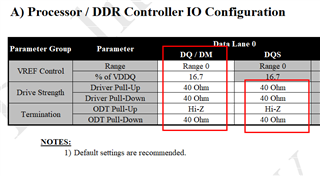
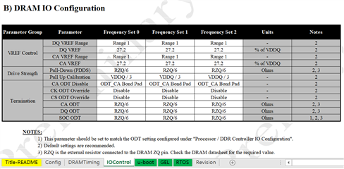
On IOControl page
---------------------------------------------------------
A) Processor / DDR Controller IO Configuration :
- Default settings are recommended.
B) DRAM IO Configuration
Assume RZQ = 240 Ohm
VREF Control
DQ VREF Range Freq Set 0 Freq Set 1 Freq Set 2
--------------------------------------------------------------------------
DQ VREF Range : Range 1 Range 1 Range 1
DQ VREF : 27.2 27.2 27.2
CA VREF Range : Range 1 Range 1 Range 1
CA VREF : 27.2 27.2 27.2
Drive Strength
Pull-Down(PDDS) : RZQ/6 RZQ/6 RZQ/6
Pull Up Calibration: VDDQ/3 VDDQ/3 VDDQ/3
Termination
CA ODT Disable : ODT_CA Bond PAD
CK ODT Override : Disable Disable Disable
CS ODT Override : Disable Disable Disable
CA ODT : RZQ/6 RZQ/6 RZQ/6
DQ ODT : RZQ/6 RZQ/6 RZQ/6
SOC ODT : RZQ/6 RZQ/6 RZQ/6
The memory specs are below.
- Originally Used DDR : 32Gb Micron / MT53D1024M32D4DT / 64Mb x 16DQ x 8 banks x 2 channels x 2 ranks
- Newly Changed DDR : 16Gb Hynix / H54G46BYYPX053 / 64Mb x 16DQ x 8 banks x 2 channels x 1 ranks (1CS)
6888.Automotive_DA 16Gb LPDDR4_H54G46BYYV(Q,P)X053_Rev1.1.pdf
Let me add further question on the reply. Thanks
Regards,
Jack