This thread has been locked.
If you have a related question, please click the "Ask a related question" button in the top right corner. The newly created question will be automatically linked to this question.
Dear experts,
I'm trying to use TDA4VM to output DSI super frame to the UB948 screen for display. (Screen resolution is 1920*720@60Fps)
The background is:
1.TDA4VM output super frame: 1920*720@60Fps.
2.UB941 works in Left/Right 3D Splitter mode.
3.Only FPD Link port0 is connected with UB948, port1 is not connected to any device because there is only one screen.
The current update is:
1.The Screen(UB948) can display the color bar image output by UB941 which configured with internal clock and timing in Pattern mode.
2.The Screen can't display anything when UB941 is configured to use external timing. And the value read from the indirect register DSI_VC_DTYPE(0x2A) of UB941 is 0x00.
This phenomenon seems to be consistent with the example in section 4.2 of the DS90UB941AS-Q1 DSI Bringup Guide.pdf
The question is :
1.How can I configure TDA4 DSS to "enter Low Power Mode at least once per frame during one of the available BLLP periods" ?
2. Is there any problem If I only connect the fisrt port of FPD Link when UB941 is in splitter mode?
More information is shown below:
1. Configuration of UB941:
uint8_t Ub941Config[][3] = {
/*
* CMS Display
* 1920*720*2@60Fps
* HSW = 16 * 2
* HFP = 72 * 2
* HBP = 72 * 2
* VSW = 2
* VFP = 19
* VBP = 19
* PCLK= 95 * 2
*/
{0x1a, 0x01, 0x08}, // Disable the DSI inputs
{0x1a, 0x06, 0x00}, // Read Deserializer ID
{0x1a, 0x1E, 0x01}, // Select FPD-Link Port 0
{0x1a, 0x03, 0x9A}, // Enable Pass-Through, Enable CRC Cheker, Enable Filter, Enable auto-switch
{0x32, 0x20, 0x99}, // Set 948 to lighte screen
{0x32, 0x21, 0x09}, // Set 948
{0x1a, 0x1E, 0x01}, // Select FPD Link port 0
{0x1a, 0x4F, 0x8C}, // Set Continuous DSI clock mode, Single-DSI mode, DSI Input port 0, 4Lanes
{0x1a, 0x5B, 0x07}, // Select Force Splitter mode
{0x1a, 0x56, 0x80}, // Enable Left/Right 3D processing, Select DSI Reference Clock Mode
{0x1a, 0x32, 0x80}, // Set the line size to 1920(LSB)
{0x1a, 0x33, 0x07}, // Set the line size to 1920(MSB)
// Crop Port0 1920*720 image
{0x1a, 0x1E, 0x01}, // Select FPD-Link Port 0
{0x1a, 0x36, 0x00}, // Set crop start X position to 0(bit[0:7])
{0x1a, 0x37, 0x80}, // Set crop start X position to 0(bit[8:12]) and enable cropping
{0x1a, 0x38, 0x7F}, // Set crop stop X position to 1919 (LSB)
{0x1a, 0x39, 0x07}, // Set crop stop X position to 1919 (MSB)
{0x1a, 0x3A, 0x00}, // Set crop start Y position to 0 (LSB)
{0x1a, 0x3B, 0x00}, // Set crop start Y position to 0 (MSB)
{0x1a, 0x3C, 0xCF}, // Set crop stop Y position to 719 (LSB)
{0x1a, 0x3D, 0x02}, // Set crop stop Y position to 719 (MSB)
// Crop Port1 1920*720 image
{0x1a, 0x1E, 0x02}, // Select FPD-Link Port 1
{0x1a, 0x36, 0x00}, // Set crop start X position to 0(bit[0:7])
{0x1a, 0x37, 0x80}, // Set crop start X position to 0(bit[8:12]) and enable cropping
{0x1a, 0x38, 0x7F}, // Set crop stop X position to 1919 (LSB)
{0x1a, 0x39, 0x07}, // Set crop stop X position to 1919 (MSB)
{0x1a, 0x3A, 0x00}, // Set crop start Y position to 0 (LSB)
{0x1a, 0x3B, 0x00}, // Set crop start Y position to 0 (MSB)
{0x1a, 0x3C, 0xCF}, // Set crop stop Y position to 719 (LSB)
{0x1a, 0x3D, 0x02}, // Set crop stop Y position to 719 (MSB)
// Program TSKIP_CNT DSI parameter on DSI Port0
{0x1a, 0x40, 0x04}, // Select Indirect register access to DIS Port 0 registers
{0x1a, 0x41, 0x05}, // Select DPHY_SKINP_TIMING register
{0x1a, 0x42, 0x40}, // Write TSKIP_CNT value for 2*47.5 = 95 MHz DSI clock frequency, Round(95*2*3*65/1000 - 5) = 32
#if 1
{0x1a, 0x40, 0x10}, // Select DSI/D-PHY Analog Indirect Registers
{0x1a, 0x41, 0x86}, // Set Indirect register addr to DSI0_CLK_INVERSION
{0x1a, 0x42, 0x0A}, // Set DSI0_CLK_INVERSION Register, Inverted sampling clock (normal operation)
{0x1a, 0x41, 0x94}, // Set Indirect register addr to DSI1_CLK_INVERSION
{0x1a, 0x42, 0x0A}, // Set DSI1_CLK_INVERSION Register, Inverted sampling clock (normal operation)
#endif
{0x1a, 0x1E, 0x01}, // Select FPD-Link Port 0
{0x1a, 0x40, 0x04},
{0x1a, 0x41, 0x20}, // Select DSI_CONFIG_0
{0x1a, 0x42, 0x6F}, // Don't regenerate orignal VS/HS Timing
{0x1a, 0x01, 0x00}, // Enable the DSI inputs
};
2.DSI timing configuration at SOC:
#if def ENABLE_DSS_DSI
prm.display_type = APP_DSS_DEFAULT_DISPLAY_TYPE_DSI;
prm.timings.width = 2*1920U;
prm.timings.height = 720U;
prm.timings.hFrontPorch = 2*72U;
prm.timings.hBackPorch = 2*72U;
prm.timings.hSyncLen = 2*16U;
prm.timings.vFrontPorch = 19U;
prm.timings.vBackPorch = 19U;
prm.timings.vSyncLen = 2U;
prm.timings.pixelClock = 2*95000000ULL;
#endif
status = appDssDefaultInit(&prm);
APP_ASSERT_SUCCESS(status);
Best regards
Damon
Hi Damon,
I am sorry, i did not get the question, is this question for DSS or ub941?
DSS can be configured to output 1920x720 resolution via DSI. I can help with it.
But can you start a new thread for ub941 configuration?
Regards,
Brijesh
Hi Brijesh,
Thank you for you reply! At present, what I am confused is how to configure DSS to output a DSI video stream with a suitable resolution?
There seems to be no signal input when I detect some pins(DSI0_DxN, DSI0_DxP) on ub941 for now.
I can do the configuration of ub941 in another thead if you suggest. And can I ask why do we need a new thread? To control the power switch or for other reasons? I saw a function call inside Func:appDssDefaultInit() in File:appp_dss_defaults.c, so I put a new func instead of the older one to config ub941.
Hi Damon,
Could you please help me with below questions
- what is output resolution?
- what ls lane speed?
- how many lanes?
I can help you in DSS, but would require help from serializer team for ub941 configuration.
Regards,
Brijesh
Hi Brijesh,
My ultimate goal is to output a 2*1920*720@60Fps superframe into ub941. And I plane to use 4 datelanes. As to the lane speed I'm not sure how to caculate .
And I'll ask Sherry who helped me with ub941 configuration to join our discussion.
Hi Damon,
For this resolution, the minimum lane speed requires is around 1.2Gbps (2*1920*720*24*60*1.2). But it really depends on whether ub941 supports this lane speed.
Regards,
Brijesh
Hi Brijesh,
Thank you!
Do you mean the total speed of 4lanes should be 1.2Gbps or per lane? According to the ub941 manual, it supports the maximum rate is 1.5Gbps per lane.
I‘ve just browsed some relevant questions. Then I realised it's important to caculate the lane speed. And I'm tying to work on it.
Regards,
Damon
1.2Gbps is per lane. Since it supports 1.5Gbps, it should be ok. We should be able to support 2*1920*720 @60fps resolution with 24bit RGB output format from DSS.
Regards,
Brijesh
Hi Brijesh,
Thank you!
According to formula, the specific value of ane speed is: 2*(1920+160)*(720+40) * 24 * 60 / 4 = 1.138Gbps.
And based on the changes that have been made before, I added two more modifications:
1.Filepath: /psdk_rtos_j7/vision_apps/utils/dss/src/app_dss_defaults.c
Changes: dsiParams.num_lanes = 4u;//2u
2.Filepath: psdk_rtos_j7/pdk_jacinto_07_03_00_29/packages/ti/drv/dss/src/drv/dctrl/dss_dctrlDsi.c
Changes: dsiObj->dphyTxOpDiv = 0x4;//0x2;
dsiObj->dphyTxFbDiv = 0x178;
dsiObj->dphyTxRate = 0xE7;//0x1CE;
I'm I right with these changes? Are there any changes that need to be made?
Regards,
Damon
Hi Damon,
I just gave an example. According to these calculation, this is minimal lane speed required. I would suggest to keep the lane speed to 1.5Gbps, just to have some margins in case required for protocol overhead and LP/ULP states.
The changes would then be
Changes: dsiObj->dphyTxOpDiv = 0x1
dsiObj->dphyTxFbDiv = 0x138; (or 0x139)
dsiObj->dphyTxRate = (0x12 << 0) | (0x12 << 5);
Regards,
BRijehs
Hi Brijesh,
Thank you for reply!
My calculation results on datalane have just been confirmed by Sherry(an engineer in charge of the ub941 from TI). And she suggest we set 1.5Gbps for datalane too. So I tried the changes as you shared.But there still nothing happened.
Here are part of configurations in func:Dss_dctrlDrvInitDSI():
dsiObj->dphyTxIpDiv = 0x2;
dsiObj->dphyTxOpDiv = 0x1;//0x2;
dsiObj->dphyTxFbDiv = 0x139;//0x178;
dsiObj->dphyTxRate = (0x12<<0)|(0x12<<5);//0x1CE;
dsiObj->cfgDsiTx.numOfLanes = 0x2u;
dsiObj->privDsiTx.numOfLanes = 0x2u;
And I got one more qustions :At present,I have not opened another thread to configure ub941. The configuration is still in func: appDssDefaultInit().
What's your opinion about the current situation?
Regards,
Damon
Hi Damon,
From DSS perspective, the changes seems to be fine, except number of lanes. I thought you wanted number of lanes to be 4. Isn't it? Are you setting it from the application?
After these changes, you would require to rebuild PDK. Could you please make sure it is done?
There could be some changes required in ub941 configuration for 1.5Gbps lane speed, i am not sure about it. Currently, in SDK, ub941 is configured in the API appDssConfigureUB941AndUB925, in file ti-processor-sdk-rtos-j721e-evm-07_03_00_07\vision_apps\utils\dss\src\app_dss_j721e.c ? Could you please check with Sherry about configuration, make changes here and try again?
Regards,
Brijesh
Hi Brijesh,
Yes, I think the number of lanes is recovered in func: Dss_dctrlDrvSetDSIParams().
I'll re-check to see if there is a configuration error in my code. And report to you later.
Regards,
Damon
Hi Brijesh,
I have made a comprehensive examination still didn't find any configured error.
I also made some confirmation work on the three questions you mentioned above:
1、Modified DPHY parameters in func:Dss_dctrlDrvInitDSI():
dsiObj->dphyTxIpDiv = 0x2;
dsiObj->dphyTxOpDiv = 0x1;//0x2;
dsiObj->dphyTxFbDiv = 0x138;//0x178;
dsiObj->dphyTxRate = (0x12<<0)|(0x12<<5);//0x1CE;
dsiObj->cfgDsiTx.numOfLanes = 0x4u;
dsiObj->privDsiTx.numOfLanes = 0x4u;
2、After modifying the parameters of DPHY, I executed 'make sdk_scrub && make sdk'. And I also checked the timestamp of the dss_dctrlDsi.oer5f has been updated.So I think these modificaionts should be effective.
3、I confirmed with Sherry: ub941doesn't need to configure the speed of data lane.
In addition, I also tested the pins on 941, which is connected with the DSI output on the SOC. But found that the DSI0_CLKP pin is always at a high voltage state, while the DSI0_CLKN pin keeps in low voltage state.Does this mean that SOC didn't output DSI clock?
And the result of reading from DSI_VC_DTYPE(0x2A) on 941 is 0x00. It also means that 941 has not received effective DSI data.
What do you think about current issues and phenomena? And could you give me some test suggestions?
Regards,
Damon
Sorry, add a question: “Where should I configure or confirm the DSS output format RGB88?”
I saw a "obj->videoIfWidth = APP_DCTRL_VIFW_24BIT". Is this configuring the output format?
Regards,
Damon
Hi Brijesh,
I just found a register in the manual: CTRLMMR_DPHY_TX0_CTRL. It's said that it contrls controls whether DPHY-TX0 works in DSI0 mode or CSI-TX-IF0 mode. So do I need to set this register in my software? If yes, where can I find the relevant configuration parameters? Cuz I tried to find this register in the code but didn't find it
Regards,
Damon
Hi Damon,
Please find answers to your questions below.
1, Yes, it the lines are not toggling, there is not output. Have you many any other change for the DSI output? Have you enabled DSI output in app_cfg_mcu2_0.h header file and disabled CSITX?
2, DSS output is always RGB for the discrete sync, we just need to configure interface size, which is configured to 24bit using this field.
3, Yes, we need to set the control module register to use DPHY for the DSI output. This is currently taken care in the dssDctrlSetDSIInCtrlMod API in ti-processor-sdk-rtos-j721e-evm-07_03_00_07\pdk_jacinto_07_03_00_29\packages\ti\drv\dss\src\drv\dctrl\dss_dctrlDsi.c file. But it assumes that the control module registers are not unlcoked. So can you please check value at the register at the offset (0x00104300). It must be set to 0x0 to enable DSI output. As such, reset value is 0x0, so by default output is DSI.
Regards,
Brijesh
Hi Brijesh,
Yes,I checked the three points above, it's the same as you said,
And here is a good news, I use a set of parameters from another post to try to display 1280*800 DSI on my screen.And it works!
(Here is the link of the post: https://e2e.ti.com/support/processors-group/processors/f/processors-forum/1015474/tda4vm-how-to-set-dsi-dphy-div-for-2560x800-resulution/3755063?tisearch=e2e-quicksearch&keymatch=TDA4%20DSI#3755063)
But When I change the resolution to 1920*720 in SOC & 941 and replace the orignal parameters of DPHY with you provide before. It still can't show anything.So I start to doubt whether my DPHY parameters are correct:
dsiObj->dphyTxIpDiv = 0x2;
dsiObj->dphyTxOpDiv = 0x1;
dsiObj->dphyTxFbDiv = 0x138;
dsiObj->dphyTxRate = (0x12<<0)|(0x12<<5);
dsiObj->cfgDsiTx.numOfLanes = 0x2u;
dsiObj->privDsiTx.numOfLanes = 0x2u;
More importantly, I want to learn what these DPHY parameters stand for? And how to calculate? At present, I have not found related instructions in the manual.Could you please help me with this?
Regards,
Damon
Hi Damon,
Please refer to below thread for information on how to calculate these parameters.
Regards,
Brijesh
Hi Brijesh,
I've checked this post. And learned some related instructions in the manual. But I stiil have few questions:
1.Is that sure the value of IpDiv must be fixed to 0x2?
2.What does the DataRate in the following formula represent? Does it the represent the same concept as LaneSpeed or is its value twice the pixel clock?
FbDiv = ((Data Rate * 2 * OpDiv * IpDiv) / (19.2MHz))
3.I see that the TxRate corresponds to bit[9-5] and bit[4-0] in register DPHY_TX_PCS_TX_DIG_TBIT0.But I don't understand what PCS_BAND_CTL_REG_R and PCS_BAND_CTL_REG_L are used for? And How their values are calculated?
It would be great if you can please take 1920*720@60Fps(570Mbps lane speed) as an example to explain the above questions.
Regards,
Damon
Hi Damon,
1.Is that sure the value of IpDiv must be fixed to 0x2?
Yes, it is fixed in the current implementation.
2.What does the DataRate in the following formula represent? Does it the represent the same concept as LaneSpeed or is its value twice the pixel clock?
FbDiv = ((Data Rate * 2 * OpDiv * IpDiv) / (19.2MHz))
Yes, data rate is lane speed in terms of bps
3.I see that the TxRate corresponds to bit[9-5] and bit[4-0] in register DPHY_TX_PCS_TX_DIG_TBIT0.But I don't understand what PCS_BAND_CTL_REG_R and PCS_BAND_CTL_REG_L are used for? And How their values are calculated?
These bits are used to specific lane speed. Please refer to TRM for more information on these fields.
1920*720@60Fps(570Mbps lane speed)
dsiObj->dphyTxIpDiv = 0x2;
dsiObj->dphyTxOpDiv = 0x4;
dsiObj->dphyTxFbDiv = 0x1DB; /* 2 x 2 x 4 x 570 / 19.2*/
dsiObj->dphyTxRate = (0xA<<0)|(0xA<<5);
dsiObj->cfgDsiTx.numOfLanes = 0x4u;
dsiObj->privDsiTx.numOfLanes = 0x4u;
Regards,
Brijesh
Hi Brijesh,
Thak you for the answers!
I have tried those params you offered and get the screen display succeed.But I'm sorry that still confused about the value of TxRate you set.
TxRate: (0xA<<0)|(0xA<<5) = 330, but I thought we were plant to set 570 as the Data Rate.
Could you please tell more about this params?Thank you!
Regards,
Damon.
Hi Brijesh,
Thank you for providing such detailed help.
I have successfully tested many kinds of resolution to display on the screen. They have a common premise that 941 works in Single Mode.
Now I'm tring to achive my ultimate goal: Dual-Screen display, which needs 941 work to work in Splitter Moed to crop and output the SupperFrame to two DSI port..
There are two problems when the video isdisplayed on the screen:
1.The video image is black and white instead of color
2.The cropped image area is inconsistent with the configuration in the code.
Here are my code and pictures of test result:
1.Resolution, Pixel Clock, HS/VS:
prm.timings.width = 2*800U;
prm.timings.height = 600U;
prm.timings.hFrontPorch = 2*40U;
prm.timings.hBackPorch = 2*88U;
prm.timings.hSyncLen = 2*128U;
prm.timings.vFrontPorch = 1U;
prm.timings.vBackPorch = 23U;
prm.timings.vSyncLen = 4U;
prm.timings.pixelClock = 2*40000000ULL;
2.Dphy params:
/* params for 2560*720 */
dsiObj->dphyTxIpDiv = 0x2;
dsiObj->dphyTxOpDiv = 0x2;
dsiObj->dphyTxFbDiv = 0x173;
dsiObj->dphyTxRate = (0x0E<<0)|(0x0E<<5);//(0x7<<0)|(0x7<<5);
dsiObj->cfgDsiTx.numOfLanes = 0x2u;
dsiObj->privDsiTx.numOfLanes = 0x2u;
3.Pictures of resulat:
Is there any additional configuration that needs to be done when I want to output a supper frame? What's your opinion on this problem?
Regards,
Damon
Hi Damon,
I have tried those params you offered and get the screen display succeed.But I'm sorry that still confused about the value of TxRate you se
In this register, we set the left and right band speed, typically they are same. Please refer to TRM for more information.
Is there any additional configuration that needs to be done when I want to output a supper frame? What's your opinion on this problem?
This seems more to do with the ub941 configuration. Could you please check with ub941 team?
Regards,
Brijesh
Hi Brijesh,
I inadvertently solved the problem about 941 working in SplitterMode.It is related to the width & height settings of the output image of the SRV node I set:
Background, the graph of my demo is:capture -> convert -> srv -> convert -> display
1.At first, I set the width & height to 2560*720. The image displyed on the screen will be abnormal.
2.When I set it to 1920*720 or 1280*720 and hold the width & height of display image to 2560*720. The screen is displayed normally.
Although the problem has been resolved, the specific reason is not clear yet.
I checked the relevant code of the SRV node,but still don't understand why the SRV node cannot be set to 2560*720 ? How do you think about this?
Regards,
Damon
Hi Damon,
Do you mean you are able to get dual serialized output from ub941 with 1280x720 resolution? and the issue of the color is due to SRV node not able to output 2560x720 resolution? But why do you require 2560x720 resolution from SRV, when the actual display is 1280x720? Isn't ub941 going to split the frame into two halves and send them on different outputs?
We can check why SRV node does not support 2560x720 resolution, but i thought your requirement is different.
Regards,
Brijesh
Hi Brijesh,
Yes, I;m able to get dual serialized output from ub941 with1280x720 resolution.
My goal is to display 1280*720 video images on both screens. So I think the SOC should output a super frame of 2560*720.
Then I thought the width & height of output images of each node in my demo should also be 2560x720 at first.
Now I just changed the output image of SRV node from 2560x720 to 1280*720. And it displayed normally on two DSI output port.
To be honest, I'm not so sure about the width and height of the output image of these two nodes.So I want ot hear your suggestions.
Regards,
Damon
Hi Damon,
So both the displays/panels should display independent content, is this correct understanding? or do you want to display half of SRV output in one display and other half in second display?
We can do it on two ways,
1, we can change output resolution on all nodes to 2560x720 and generate single big frame to be sent out by display.
2, another ways is, we use two display pipelines, each reads 1280x720 resolution images and then using blender, we put both the inputs side by side and send it out as 2560x720 resolution.
Regards,
Brijesh
Hi Brijesh,
So both the displays/panels should display independent content, is this correct understanding?
You are right at this. I want these two screens to display video images independently.
1, we can change output resolution on all nodes to 2560x720 and generate single big frame to be sent out by display.
If we go this way, we need to solve the problem that "SRV node doesn't support' 2560*720".Or else we have to set the output image of SRV to 1280*720 or some other resoltion.
I did a set of tests and found that:
1.when I set the output image of SRV to be 2040*1080, the color displayed on the screen is normal
2.when I set the output image of SRV to be 2050*1080 or bigger, the color displayed on the screen is black and white
Can you help me solve or understand the cause of this problem?
2, another ways is, we use two display pipelines, each reads 1280x720 resolution images and then using blender, we put both the inputs side by side and send it out as 2560x720 resolution.
Am I right with this? I put two SRV nodes and Display nodes into the graph pipeline like:
|-------> SRV_0 ----> Display_0
|
Capture ----
|
|-------> SRV_1 ----> Display_1
Hi Damon,
Am I right with this? I put two SRV nodes and Display nodes into the graph pipeline like:
You could just direct SRV node's output to two display nodes, as shown below. This is possible, though both the displays will just show same SRV output, which i guess you dont want.
Capture --> SRV |----> Display0
|-----> Display1
2.when I set the output image of SRV to be 2050*1080 or bigger, the color displayed on the screen is black and white
Can you help me solve or understand the cause of this problem?
Can you check first here if the input to this display is correct? If it is not, then SRV node is not able to generate such big size image..
Regards,
Brijesh
Hi Brijesh,
You are right. I want to display two different image on two screen.This is used for CAM or TAP.
What do you mean that "if the input to this display is correct"? Actually the input image to Display is not from SRV directly. There is a Convert node between SRV and Display used to convert image format from RGBA to NV12, but without changing it's size.
And the output image of Display was fixed to 1920*1080 when I was doing those tests.The DSS output was changed to HDMI instead of DSI to exclude the influence of other factors.
So the complete informations of those test are:
test1: SRV_input(1280*720),SRV_output(2040*1080), Display_input(2040*1080), Display_output(1920*1080)
result1: video color is normal
test2: SRV_input(1280*720),SRV_output(2050*1080), Display_input(2050*1080), Display_output(1920*1080)
result2: video color is abnormal(black and white)
I think the input to display is not wrong, because it can scale the input image,right?
Regards,
Damon
Hi Damon,
I think your original question was different, you wanted to get bigger frame from DSI. I guess that is resolved, correct?
test2: SRV_input(1280*720),SRV_output(2050*1080), Display_input(2050*1080), Display_output(1920*1080)
result2: video color is abnormal(black and white)
I think the input to display is not wrong, because it can scale the input image,right?
Yeah, this looks something in the display. It can down-scale this resolution to 1920. But i am bit worried about the line width. I guess it would work till 2048. But beyond that, we would have to make some more changes in the display configuration.
Regards,
Brijesh
Hi Brijesh,
Sorry for the late reply.
Do you mean this phenomenon is related to Display node but not SRV ?
Is it possible that the Display out put the supper image(2560*720) input by SRV without any scaling?
Could you please guide me how to configure the Display?
Regards,
Damon
Hi Brijesh,
This problem is solved finally.
I'm sorry I didn't introduce the detailed graph stream to you:
Capture(YUYV) ---> Convert_1(NV12) ---> SRV(RGBX) ---> Convert_2(NV12) ---> Display
There is a Convert_2 node between SRV and Display which used to convert image format from RGBA to NV12. I added this node in a previous test to verify whether the Display node supports NV12 input. And forget to remove it after test.
So the input image of Display is NV12. When I set it's size to be 2050*1080 or 2560*720, the video displayed on the screen is grayscale.
Then I removed the Convert_2 node to let Display node receive RGBA image from SRV node directly. The video shown on the screen was always normal when I did the following tests:
test1: Set both SRV and Display 2560*720, DSS: 3840*720
test2: Set both SRV and Display 3840*720, DSS: 3840*720
test3: SRV: 2050*720, Display: 1280*720, DSS: 3840*720
Based on the above phenomenon, I have obtained two speculations:
1. When the input image is YUV format, Display doesn't support larger resolutions.
2. When the input image is RGBX format, Display supports a maxmum resolution for 4K.
I believe there are related instructions in the TRM manual, but I haven't found the exact location yet. Can you help me confirm these two speculations?
Sincerely thank you for your continued attention and pationt help on this topic, and I am glad I learned a lot from you!
Thank you
Regards,
Damon
Hi Brijesh,
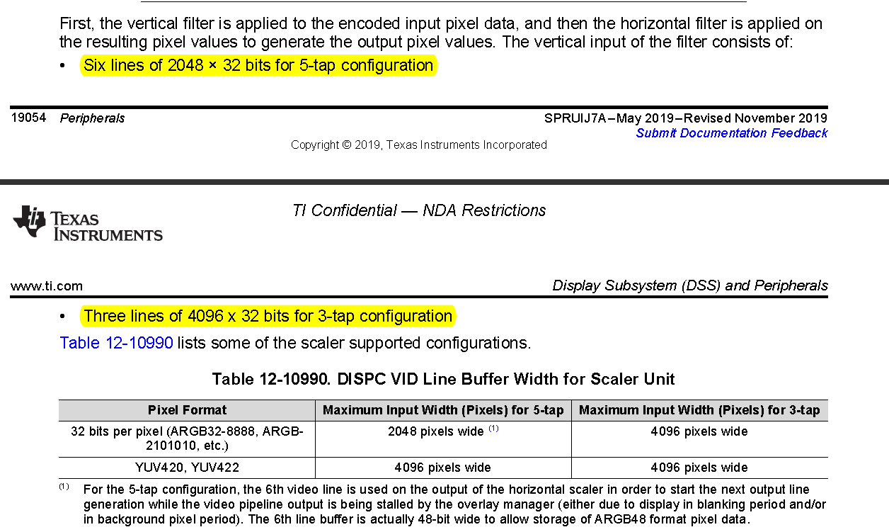
From the TRM manual I learned that the Scaler Unit in DISPC_VID moudle supports YUV420 format input image with a maximum width of 4096 pixels. As shown below:
So my guess may be wrong! But I can't figure out it. What's do you think?
1. When the input image is YUV format, Display doesn't support larger resolutions.
Regards,
Damon
Hi Damon,
Sorry for the late reply.
I this this is limitation due to 5-tap filter. can try changing to 3-tap filter and see if it works fine for NV12 format?
Regards,
Brijesh
Hi Brijesh,
I don't get it.
According to the document description, I only saw the limitations of 3-taps and 5-taps on the NV12 format. How does it affect the NV12 format?
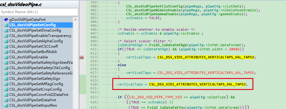
I found only one palce to configure the filter:
File: psdk_rtos_j7\pdk_jacinto_07_03_00_29\packages\ti\csl\src\ip\dss\V4\priv\csl_dssVideoPipe.c.
API: CSL_dssVidPipeSetConfig()
Can you please tell me the specific operation to modify the 3-taps filter?
Regards,
Damon
Hi Damon,
I totally agree that for NV12/yuv422 format, the line limit is 4096 for both 5-tap and 3-tap filter. But for other formats, there is different of line limit for 5-tap filter and 3-tap filter. 3-tap filter provides more line width, so wanted to just try it out.
Unfortunately, there is no driver interface to set the vertical taps, you would have to directly update registers to change this settings.
Regards,
Brijesh
Hi Brijesh,
I see. I'll take some time to do some tests latter.
Sorry I accidentally selected "this resolved my issue" by mistake.
Regards,
Damon
Hi Brijesh,
I made changes in the API: CSL_dssVidPipeSetConfig() of csl_dssVideoPipe.c file.
I added a line to set the filter mode.
Test1: I set the input image format to be RGBA and size to be 2560*720.Tested the 5-taps and 3-taps modes separately.And didn't find any difference.
Test2: I set the input image format to be NV12 and size to be 2560*720. Tested the 5-taps and 3-taps. And didn't find any difference too.
Do you have time to reproduce this issue and trace the cause?
Regards,
Damon
Hi Damon,
I really do not have setup to check large resolution.
I guess you are atleast unblocked and are able to display this resolution with the RGBA format.
Regards,
Brijesh
Hi Brijesh,
You are right. I've achieved my original purpose.Just curious to figure out this problem.
Thank you for help. I'll record this problem to avoid making mistakes in the future.
Regards,
Damon
Thanks Damon. Closing this thread.
Please start a new thread on NV12 limitation on line size.
Thank you.
Regards,
Brijesh