


Other Parts Discussed in Thread: TDA4VM
We are using TDA4VM-HS SoC in our production, but we found few board has DDR read/write error issue.
The TDA4VM is HS and need security key, we found some board has Authentication failure issue when write the Image from OSPI to DDR, and we implement some code to check the check-sum of data at OSPI and check the checksum of data transferred to DDR. Then we compare the two check-sum, we found the two check-sum result is different in the Authentication failure board, and we see the two check-sum are same at Authentication passed board.
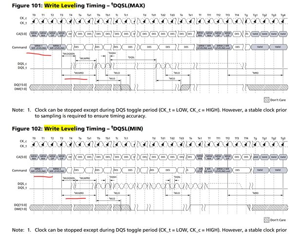
This issue should from DDR controller Write leveling configuration optimization. Need TI to help us to fin-tune Read Leveling and Write Leveling since we use the DDR controller configuration from reference design board, we need to fine tune it for massive production to avoid some board Failure due to read/write margin is just in the edge.
Also help us to check if the DDR initial configuration is optimized or not, we also see the DQS/DQ output level is incorrect: when in idle mode, the DQ/DQS is high, by normal case, during idle mode the DQ/DQS
should be low. see our other E2E case link:
