Part Number: TMS320C6678
Hi,
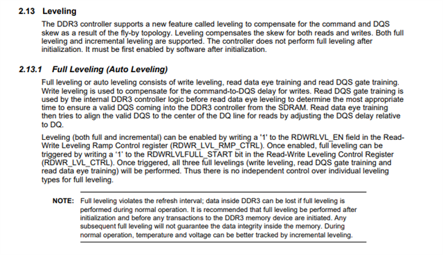
My customer using the C6678 are experiencing issues with DDR3 read access during pre-shipment testing.
The one test pattern include such as "walking test", "marching test", etc..
This single test performs hundreds of millions of write/read accesses and takes about 20hours to be done.
The problem occurs mostly in "walking test", and when the problem occurs,
when "1" is written, "0" is read, and when the same address is read continuously, "1" is read correctly,
so we think it is a memory read issue.
The frequency of occurrence of the problem is once at room temperature, and more than 300 times
when the temperature is raised to about 50°C.
Two C6678(DSP#1,DSP#2) are mounted on their customer board and each DSP are connected to four 16bit DDR3(total 64bit).
The issue occured only at 1bit of byte lane #6 or #7 of DSP#1.
This board has been mass-produced for several years, and the DDR3 peripheral layout has been done according to
TI's design guide, and since this problem has not occurred so far, we believe there is no problem with the layout design.
For now, they are using partial leveling of DDR3.
But there are above issue, so the customer are thinking to try full leveling.
With that in mind, they have the following questions.
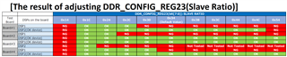
Q1.The customer want to know the details of each parameter of leveling register which are
defined in spead sheet "DDR3 PHY Calc v11" such as DATAx_WRLVL_INIT_RATIO, DATAx_GTLVL_INIT_RATIO,
RD_DQS_SLAVE_RATIO, WR_DQS_SLAVE_RATIO, WR_DATA_SLAVE_RATIO, FIFO_WE_SLAVE_RATIO.
They want to know what kind of process will be done by using these parameters.
Q2.The customer are trying to adjust the above parameter after calculated by the spread sheet.
And they want to know which parameters to adjust for a problem like this.
Q3.Is there a register that allows me to check how the initial value of each register calculated
in the spreadsheet has changed after leveling?
Q4.We would like to know about configuration flow to use full leveling.
Is configuration flow of full leveling same as partial leveling?
In full leveling, is it just that there is no setting to enter the fixed value(0x200) to DDR3_CONFIG_REG23
that was recommended in the partial leveling?
Q5.To use full leveling, I guess incremental leveling are needed after full leveling because
of errata advisory 9 workaround 3.
In Keystone I DDR3 Initialization(sprabl2e) page.16, it said as follow:
********************************************************************************
Example 25. Incremental Leveling After Full Automatic Leveling
RDWR_LVL_RMP_WIN = 0x00000502;
RDWR_LVL_RMP_CTRL = 0x80030300;
RDWR_LVL_CTRL = 0x7F090900;
********************************************************************************
Does this setting mean workaround 3 of advisory 9 ?
best regards,
g.f.