This thread has been locked.

If you have a related question, please click the "Ask a related question" button in the top right corner. The newly created question will be automatically linked to this question.

AM4378: Confirmation about power-up sequence

Part Number: AM4378
Other Parts Discussed in Thread: TPS65218D0

Hi,.

A customer of ours is building a custom board using the AM4378.

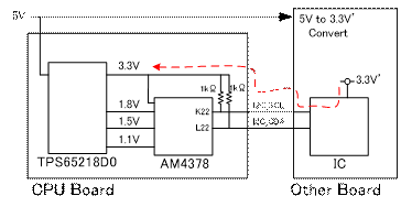
In the board they are currently building, the power is supplied from the PMIC (TPS65218D0) to the CPU (AM4378).

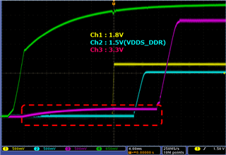
AM4378 does not use RTC, and IO voltage is used under the condition of 2 voltages (3.3V and 1.8V), so it should be activated in the order of 1.8V → VDDS_DDR(1.5V) → 3.3V as shown below from the power-up sequence (Figure 5-7.) described in the data sheet.

After checking the waveforms of the board they created, as shown in the figure below, the order in which the specified voltage of each power supply is reached is as required: 1.8V → VDDS_DDR(1.5V) → 3.3V, but in the area enclosed by the red dashed line, the voltage is reached via IO (I2C interface) with another board → PU resistor for I2C (1k The red dashed line indicates that the voltage is increased by about 0.25V for a period of 24ms due to the power supply sequence to the AM437x.

Please confirm if there is a problem with the power supply sequence to AM437x.

Best Regards,

Kouji Nishigata

  • Hello Kouji Nishigata.

    Thank you for the query.

    I have a few questions

    the voltage is reached via IO (I2C interface) with another board → PU resistor for I2C (1k

    Can you please share some inputs on the I2C interface used and the connections.

    I assume the pink line is the 3.3V.

    Help \me understand the green trace please.

    Regards,

    Sreenivasa

  • Hi Sreenivasa,

    Thanks for your reply.

    Yes, the pink line is 3.3V (the letters in red in the diagram are wrong).
    What do you need to know about the I2C interface?
    I believe the green line is VIN_BIAS, but I am checking just to be sure.
    The customer does not seem to want to change the board much and they want to know about possible problems with this sequence.

    Best Regards,

    Kouji Nishigata

  • Hello Kouji Nishigata.

    Thank you for the input.

    The i2C interface does not seem to be fail safe. So i am trying to understand  the I2C interface connection from processor to attach device and the pullup source.

    The USB0_VBUS, USB1_VBUS, and DDR_RESETn are the only fail-safe IO terminals. All other IO terminals are not fail-safe and the voltage applied to them should be limited to the value defined by the Steady State Max. Voltage at all IO pins parameter in Section 5.1.

    Regards,

    Sreenivasa

  • Hi,

    I received a block diagram from a customer regarding I2C. The Othre Board is made by another company. PullUp of I2C interface is specified to be done on the CPU Board side.

    As for the OtherBoard, there is no circuit diagram, so I am guessing, but it is used after converting the supplied 5V to 3.3V.

    ! [img](file:///C:/Users/090738/AppData/Local/Temp/msohtmlclip1/01/clip_image002.gif)

    Both of these boards are supplied 5V at the same time, but the 3.3V on the OtherBoard seems to start up faster and I believe the potential is rising through the I2C line.

    For the K22/L22 pins that are connected, we believe that the BALL RESET STATE is high impedance according to the Pin Attributes in the DataSheet, and we want to confirm that there is no problem if the timing is as previously indicated.

    Best Regards,

    Kouji Nishigata

  • Hello Kouji Nishigata,

    Thank you for the inputs.

    I assume the i2C interface on the other board is open drain and has pulls.

    We are recommending powering the processor and the attached devices from the same power supply.

    Try removing the pulls on K22/L22 for testing.

    This configuration is not recommended for implementation.

    Regards,

    Sreenivasa

  • Hi, Sreenivasa

    Thanks for the reply.

    I will ask the customer if I can remove the K22/L22 and see the levels.

    They just want to product with the board as it is and want to hear what problems there would be with the board as it is.

    Also, the OtherBoard is made by another company and cannot be changed. If there is a problem that cannot be overlooked in this situation, they are thinking of shifting the timing of the 5V power supply to the OtherBoard. However, this 5V supply is also not through the CPU Board, so it will require a lot of changes.

    Best Regards,

    Kouji Nishigata

  • Hello Kouji Nishigata,

    Thank you.

    The AM437x IOs are not fail-safe and the interface that you have shown is not a valid use case that has been tested.

    The issues could be functional failures and reduced device reliability or operational life.

    Regards,

    Sreenivasa

  • Hi, Sreenivasa

    Thanks for the reply.

    Regarding the voltage of the I2C interface (Typo for IOS?), the actual measurement in the diagram is about 0.25V, which does not seem to exceed the value listed in the DataSheet, but could it still be a problem?

    The customer has started consulting with the manufacturer of the OtherBoard, but it seems that they would like to avoid having the commercial product modified, as this would be a factor that would increase the cost.

    Best Regards,

    Kouji Nishigata

  • Hello Kouji Nishigata,

    Please help me understand which parameter in the datasheet you are referring.

    the actual measurement in the diagram is about 0.25V, which does not seem to exceed the value listed in the DataSheet, but could it still be a problem?

    Regards,

    Sreenivasa

  • Hi, Sreenivasa

    Thanks for the reply.

    Regarding the 0.25V, it was the actual value of the 3.3V line in the oscilloscope diagram I wrote in my first question, but the I2C interface is through a pull resistor, so it could be more than that.
    Would it be better to have the customer measure the I2C pin?
    Also, as for the standard, I think it can withstand about 0.3 V by looking at the line "-0.5 V to IO supply voltage + 0.3 V" in the table "Steady State Max. Voltage at all IO pins" in chapter 5.1. Please point out if I am looking in the wrong place.

    Best Regards,

    Kouji Nishigata

  • Hello Kouji Nishigata,

    Thank you for the inputs.

    The voltage that you mentioned is: Steady State Max. Voltage at all IO pins(5) –0.5 V to IO supply voltage + 0.3 V

    This assumes IO supply is available.

    We do not allow any current (Injection current) on the IOs. These could affect the long term reliability. It depends on many factors including the duration the current is seen. 

    Any thoughts on the pull used on the other board that is interfaced.

    Regarding the 0.25V, it was the actual value of the 3.3V line in the oscilloscope diagram I wrote in my first question, but the I2C interface is through a pull resistor, so it could be more than that.
    Would it be better to have the customer measure the I2C pin?

    Would be good for information and further discussion.

    Regards,

    Sreenivasa

  • Hi, Sreenivasa

    Thanks for your answer.

    At one point I confused the supply voltage with the voltage of the I2C port, which confused the conversation.
    After talking to the customer, we have decided to work around the current draw from the I2C interface with a hardware change.
    They haven't decided on a concrete plan yet, but let me close this time.

    Best Regards,

    Kouji Nishigata

  • Hello Kouji Nishigata,

    Thank you for the inputs.

    Regards,

    Sreenivasa