Hi TI Experts,
I have the below queries regarding implementation of USB interface
1. Supported USB interface configuration
2. Is VBUS connection required for Host configuration or Device configuration
3. Can I have the VBUS supply input connected when the SoC power supply is switched off
4. Is there a power sequencing requirement for VBUS
5. Can I connect 5V input from the USB connector directly to VBUS
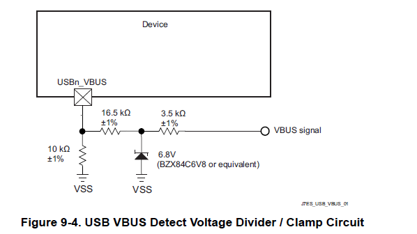
6. Recommended VBUS supply voltage divider
7. SOC VBUS input voltage range and Zener diode connection
8. Supported USB Backup bootmode configuration.
9. Recommended USB RCALIB resistor
10. How to deal with the USB unused pins
11. Is the USB0_ID connection required for Host configuration or Device configuration.
12. Power supply switching and protection when the SOC is configured as USB Host
13. Are these recommendations valid for other Sitara processors or MCUs?
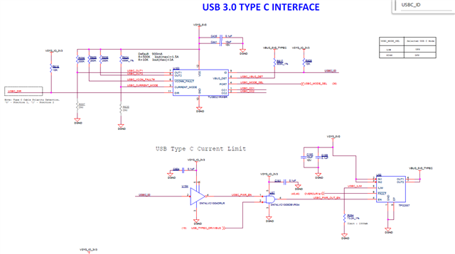
14. Do you have some recommendations on the Type-C implementation.
15. Can I use 3.4K instead of 3.5K.
16. Do the differential signal pins (oLDI, USB, etc.) have the capabilities to adjust the swing of the voltage?
Let me know your thoughts.
Hi Board designers,
USB0 interface supports Host or Device or Dual-Role (DRD)
VBUS connection for Host interface is optional.
It is recommended to connect the VBUS when the USB interface is configured as Device.
The recommended voltage range is the divided voltage equivalent of 4.75 V - 5.25 V for normal operation.
USB VBUS IO is fail-safe. The VBUS input does not have any dependency on the SOC power supply.
USB VBUS IO is fail-safe and do not have any sequencing requirements.
VBUS pin cannot be connected directly to external/connector VBUS, as IO is not 5 V compliant. Recommend using voltage divider and/or current limiter to ensure IO requirements are met. VBUS pin can be consider fail-safe only if recommended external divider circuit is used.
Connection of 3.3 V directly to VBUS input is not allowed or recommended.
For USB Device interface, it is recommended to connect a switched external USB VBUS supply to the USB0_VBUS input of the SOC through recommended resistor divider.
Refer section 9.2.3 USB VBUS Design Guidelines of the data sheet.
We do not define VBUS thresholds. VBUS thresholds are defined in the USB specification. The thresholds were designed to be compliant to the USB specifications and validated via USB-IF compliance tests.
The VBUS input has an ESD clamp to the 3.3 V rail. The USB VBUS Design Guidelines section of the datasheet defines the VBUS connection topology. This voltage divider / clamp circuit allows VBUS to go up to 30 V without harming the VBUS input. The Zener diode could be removed and a 20 KΩ resistor could be substituted for the 16.5 KΩ and 3.5 KΩ resistors if your system will never apply a VBUS potential greater than 5.5 V and the 5.5 V is sourced on-board.
USB0 interface is recommended to be configured as a device. USB DFU backup mode works with 0.75 V SOC core supply.
Refer below section of the data sheet.
6.3.25 USB, 6.3.25.1 MAIN Domain, Table 6-79. USB0 Signal Descriptions
RCALIB resistor should not exceed ±1% at any operating condition for the lifetime of the product.
Refer below section of the data sheet.
6.4 Pin Connectivity Requirements, Table 6-80. Connectivity Requirements
It is recommended to connect USB0_ID pin to VSS through a 0 Ω resistor when the USB interface is configured as Host.
It is recommended to leave the USB0_ID pin floating when the USB interface is configured as Device.
For implementations that do require DRD functionality, connect USB0_ID pin directly to the corresponding ID pin on a USB Micro-AB connector. Depending on the cable attached, the USB0_ID pin will be terminated, and the processor will be configured as Host or Device.
USB0_DRVVBUS can be used to control the power (load) switch. The USB interface or the Linux driver is not checking the status of VBUS to determine if there is a fault condition. In that case, you should connect the fault output of the VBUS power (load) switch to a GPIO and configure the GPIO to generate an interrupt that indicates there has been an over-current condition.
The recommendations are valid for the following family of devices:
AM243x
AM64x EVM or SK does not have the implementation.
Refer below starter kit for implementation.
It should be Ok to use a 3.4K for the divider. It is recommended to select 3.48K value based on the availability.
16. Do the differential signal pins (oLDI, USB, etc.) have the capabilities to adjust the swing of the voltage?
No.
Note:
Ensure the recommended capacitors are provided for the VBUS supply near to the connector (Host > 120 uF and Device (1-10 uF))
USB0_DRVVBUS has an internal pulldown enabled by default.
Refer below documents during the USB interface design.
Hardware Design Guide for AM6442, AM6422, AM6412 and AM2434 Processors
Hardware Design Guide for AM64x/AM243x Devices (Rev. A) (ti.com)
AM6442, AM6422, AM6412 and AM2434 Schematic Design and Review Checklist
AM64x/AM243x Schematic Review Checklist (Rev. B)
Regards,
Lavanya M R.
Hi Board designers,
Additional inputs regarding USB RCALIB resistor implementation:
The IP specification TI received from the USB PHY design team defined a 500 ohm +/-1% calibration resistor. A few weeks ago another customer reminded us 500 ohms is not a standard value for 1% resistors. They were having problems sourcing a 500 ohm +/-1%, so asked if the could use a 499 ohm +/-1% resistor.
I ask the USB PHY team if we could change the recommendation from 500 ohm +/-1% to 499 ohm +/-1% to make resistor selection easier for our customers. They confirmed this would be okay, so we changed the recommendation in the datasheet.
I assume your board has two 1 kohm +/-1% resistors connected in parallel, and you are asking if this will be okay. This should be okay since the USB PHY was initially designed for a 500 ohm +/-1% resistor.
Regards,
Sreenivasa
Hi Board designers,
Refer below section of the TRM for information related to USB2 polarity revu
• USB2 PHY:
– Fully compliant with UTMI+ Level 3 specification revision 1.0
– Supports high-speed (480 Mbps), full-speed (12 Mbps) and low-speed (1.5 Mbps) data rates
– Supports battery charging BC1.2v specification
– Supports host, peripherals and OTG 2.0 (dual role device) applications
– Supports D+/D- lane reversal for flexible board integration
– Supports USB low-power states; namely, suspend and link power management (LPM)
– Supports internal comparators for monitoring OTG voltage thresholds
– Supports multiple PLL reference clocks
– Supports internal PLL for high-speed (480 MHz) clock and data recovery (CDR) operation
– Integrated termination resistors (45 Ω, 1.5 KΩ, and 15 KΩ)
– Supports built-in self-test (BIST) for production testing
– 3.3-V ESD support on VBUS
Regards,
Sreenivasa