Hi TI Experts,
I have the below queries on using the SERDES in my design.
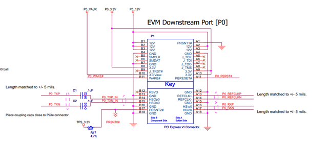
1. Supported Interfaces
2. Implementation Reference for PCIe
3. Implementation Reference for USB3.0
4. Can i use PCIe and USB3.0 interface at the same time
5. Is AM64 able to change PCIE driving? If yes, how to do?
Let me know your thoughts.
Hi Board designers,
1. Supported Interfaces
PCIe 1x Single Lane Gen 2
1x USB 3.1 DRD
USB SuperSpeed and PCIe share a common SerDes PHY. Therefore, USB will be limited to non-SuperSpeed modes when using the
SerDes PHY for PCIe.
2. Implementation Reference for PCIe
Refer TMDS64EVM, AM64x evaluation module for Sitara processors
https://www.ti.com/tool/TMDS64EVM
3. Implementation Reference for USB3.0
SK-AM64B, AM64B starter kit for AM64x Sitara processors
https://www.ti.com/tool/SK-AM64B
4. Can i use PCIe and USB3.0 interface at the same time
The use of USB3.0 and PCIe interface are mutually exclusive (USB3.0 or PCIe). USB3.0 and PCIe
cannot be used at the same time.
5. Is AM64 able to change PCIE driving? If yes, how to do?
There is no support for PCIe swing tuning.
6. I see the clock generator used in the AM64x EVM mentioned as NRND. Any thoughts ?
Refer below E2E thread
Regards,
Sreenivasa
Hi Board designers,
SERDES0 inputs are not fail-safe.
If clock or data inputs are available before the SOC supply ramps, VDDR_CORE rail could be affected causing booting issues based on the power architecture implementation.
Refer below E2E.
Regards,
Sreenivasa
Hi Board designers,
Note on Errata i2326
My customer is inputting non-SSC refclk from external source.
Is there any way they can find out if this errata does not apply to them?
Refer below E2E
Regards,
Sreenivasa
Hi Board designers,
Additional inputs regarding USB3.0
For configuring SERDES0 for USB3.0 interface as a host, refer SK-AM64B, PROC100A
https://www.ti.com/tool/SK-AM64B
USB3 interface configuration
Can an A53 core-controlled USB interface be only a USB 3.0 host, not a USB 3.0 device at the 5Gbps rate?
USB3.0 in device mode is not support, only USB2.0 in device mode is support.
Refer TRM section
USB chapter - table 12-2531
Regards,
Sreenivasa
Hi Board designers,
Refer below inputs regarding SERDES0 use case.
We have a desire to use the SERDES as a raw interface without a protocol on top. The idea would be to just run 8b/10b and limit our packet size to 10 -40 bits. Is this possible or do we need to run PCIE or USB using the PCS?
-
Regards,
Sreenivasa
Hi Board designers,
Refer below inputs regarding SERDES0 use case - contd..
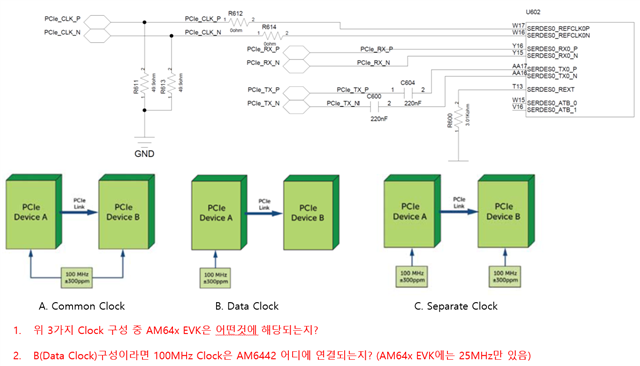
AM6442: AM64 PCIe REFCLK
AM6442: Serdes input clock (SERDES0_REFCLK)
https://e2e.ti.com/support/processors-group/processors/f/processors-forum/1364387/am6442-serdes-input-clock-serdes0_refclk
Q1: Yes, the EVM is operating in HCSL mode. HCSL clocking is required when operating in clock-input mode.
Q2: Yes, this SoC can source the 100MHz PCIe bus clock. Please note that this only applies to PG2.0. Refer to the silicon errata for more details.
Q3: This table is SerDes specific It means that the SerDes itself can operate as-described when provided any one of clock frequencies, but in the case of AM64xx, the only supported frequencies are 25MHz (internally clocked) and 100MHz (externally clocked).
PCIe reference clock termination
https://e2e.ti.com/support/processors-group/processors/f/processors-forum/1178906/tda4vm-pcie-reference-clock-termination
TDA4VM reference clock pins as outputs, so does TDA4VM clock driver require the 50ohm termination? (HCSL compatible differential input is expected at receiver)
Yes, each signal should have 50-ohm resistor to GND near the source (TDA4VM).
Applicability of LP-HCSL
https://e2e.ti.com/support/processors-group/processors/f/processors-forum/1385903/am5746-applicability-of-lp-hcsl
LP-HCSL is OK as long as it meets the PCIe Refclk specifications. Also, unlike HCSL, LP-HCSL integrates the termination resistors into the buffer so that they are not required to be placed on the PCB.
SERDES REFCLK & PCIE CLK HARDWARE DESIGN
https://e2e.ti.com/support/processors-group/processors/f/processors-forum/1376467/tda4vh-q1-serdes-refclk-pcie-clk-hardware-design/
LPHCSL output can be used to drive a HCSL input. The LP-HCSL spec was developed to be signal level compatible with HCSL so that the RX side doesn’t know the difference.
It is recommended to drive 1:1, one LPHCSL output to one HCSL receiver. close this thread.
TDA4 serdes REFCLK
https://e2e.ti.com/support/processors-group/processors/f/processors-forum/1062475/tda4vm-tda4-serdes-refclk
SERDES0_REFCLK Termination when used as Input
https://e2e.ti.com/support/processors-group/processors/f/processors-forum/1073497/dra821u-serdes0_refclk-termination-when-used-as-input
SERDES REFCLOCK (PCIe) Reference Clock Input Characteristics
https://e2e.ti.com/support/processors-group/processors/f/processors-forum/1082419/dra821u-serdes-refclock-pcie-reference-clock-input-characteristics
AC coupling and biasing
https://e2e.ti.com/support/clock-timing-group/clock-and-timing/f/clock-timing-forum/1110905/cdci6214-ac-coupling-and-biasing
PCIe reference clock termination
https://e2e.ti.com/support/processors-group/processors/f/processors-forum/1178906/tda4vm-pcie-reference-clock-termination
Heterogenous multiprocessor design - clock generator synchronisation
https://e2e.ti.com/support/processors-group/processors/f/processors-forum/1301716/tda4ve-q1-heterogenous-multiprocessor-design---clock-generator-synchronisation/
Rising/falling time failed for HCSL output
https://e2e.ti.com/support/clock-timing-group/clock-and-timing/f/clock-timing-forum/1191081/lmk03318-lmk03318---rising-falling-time-failed-for-hcsl-output
CDCI6214RGE vs CDCE6214RGE: What are the differences?
https://e2e.ti.com/support/clock-timing-group/clock-and-timing/f/clock-timing-forum/1409617/cdci6214-cdci6214rge-vs-cdce6214rge-what-are-the-differences/
LP-HCSL vs HCSL
https://e2e.ti.com/support/clock-timing-group/clock-and-timing/f/clock-timing-forum/1015683/cdce6214-lp-hcsl-vs-hcsl
From output level perspective, there's no difference. LP (Low Power)-HCSL, by its name, is more power saving. Also, there's internal 50Ohm termination for LP-HCSL so no need for external termination. Traditional HCSL may or may not have internal 50Ohm.
Common mode voltage of HCSL output
https://e2e.ti.com/support/clock-timing-group/clock-and-timing/f/clock-timing-forum/1302140/cdce6214-q1-common-mode-voltage-of-hcsl-output/
LP-HCSL is typically defined in terms of min and max swing and a single-ended crossing voltage (in place of a common mode voltage), per the PCIe specification. This single-ended crossing point voltage is between 250 mV and 550 mV.
Termination for HCSL output to input of LMK00725
https://e2e.ti.com/support/clock-timing-group/clock-and-timing/f/clock-timing-forum/1118844/lmk00725-termination-for-hcsl-output-to-input-of-lmk00725
HCSL Output pin state when disabled
https://e2e.ti.com/support/clock-timing-group/clock-and-timing/f/clock-timing-forum/1373376/lmk5b33216-hcsl-output-pin-state-when-disabled
Can I use HCSL signal as clock input?
https://e2e.ti.com/support/data-converters-group/data-converters/f/data-converters-forum/1353002/adc3562-can-i-use-hcsl-signal-as-clock-input/
800mV is single-ended so is 800mVp (peak). Differential of that is 1.6Vpp (peak-to-peak) so it will work.
App Note SLAAE45 – SEPTEMBER 2021, Table 2-1 PCIe Requirements
https://e2e.ti.com/support/interface-group/interface/f/interface-forum/1399454/tmuxhs4412-question-about-ti-app-note-slaae45-september-2021-table-2-1-pcie-requirements/
Regards,
Sreenivasa
Hi Board designers,
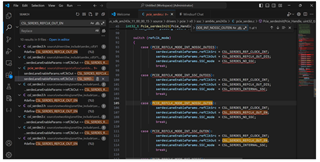
Refer below inputs regarding SERDES0 polarity reversal
12.2.3.1.1 SerDes Features
The SERDES module features include:
• Single lane PHY containing:
– Transmit and Receive I/Os
– Serializer
– Deserializer
– Clock and data recovery (CDR) unit
• Common Module (CMN)
– PLLs
– Controller bias
– Automatic calibration of pin termination resistors
– Reference clock input buffers
– Reset and startup management
• Physical Coding Sub-block (PCS)
– USB3.1 Gen 1 (5 Gbps)
•
– PCIe Gen 1 (2.5 Gbps), Gen 2 (5 Gbps)
– QSGMII Specification revision 1.2
– Symbol alignment
– Selectable serial pin polarity reversal for both transmits and receive paths
– Bit stream reordering
regards,
Sreenivasa
Hi Board designers,
Refer below inputs regarding adding external terminations when PCIe clock output from AM64x is connected to an attached device.
Regards,
Sreenivasa