Part Number: AM3354
Other Parts Discussed in Thread: TPS65218
Hello,
I am currently working on my first custom System-on-Module (SoM) design based on the AM3354 and would like to ask for a general sanity check before moving on to PCB layout.
The goal of the design is to create a flexible SoM that exposes most of the processor pins via a SODIMM connector. The intention is not to define all functionality on the module itself, but to implement most interfaces later on different carrier boards.
Current design approach:
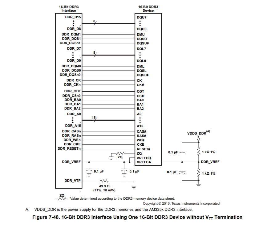
- AM3354 with external DDR3L memory
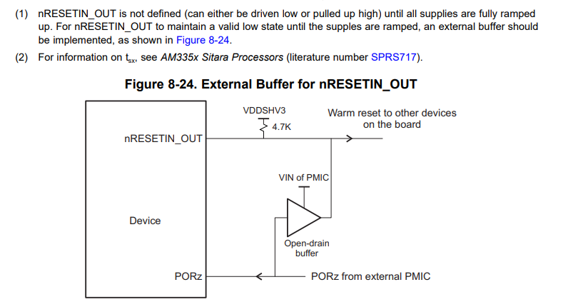
- PMIC-based power design
- Most pins routed directly to the SODIMM connector
- No fixed peripheral configuration at this stage
- Some unused pins are assigned as GND to improve signal integrity
The schematic and related design files (made in Kicad 9.07) are attached for reference . Since this is my first design of this kind, I would really appreciate any general feedback or advice. Thank you very much for your time and support.
Best regards,
Marius