Because of the Thanksgiving holiday in the U.S., TI E2E™ design support forum responses may be delayed from November 25 through December 2. Thank you for your patience.

This thread has been locked.

If you have a related question, please click the "Ask a related question" button in the top right corner. The newly created question will be automatically linked to this question.

AM335x with RMII Ethernet Phy

Other Parts Discussed in Thread: TLK110, TLK105, TLK106, SN74LVC1G34, TLK100, AM3352

Do you have an example design of AM335x connected to a 10/100 Phy using RMII interface. What I am wondering is whether the Phy or the CPU is supossed to provide the 50MHz clock. Advisory 1.0.16 in the AM335x Errata states that its output clock doesn’t comply with requirements of external RMII phy.

Will this be fixed in Rev 2 silicon?

  • No.  This will not be fixed.  The change required to fix this issue would be a major re-design of the clocking architecture.

    However, we are changing the default state of the AM335x RMII Reference Clock output to be disabled at reset.  The default state used in silicon revision 1.0 would cause the output to be enabled as soon as the ROM code tried to use RMII to boot from Ethernet.  This issue is described in Advisory 1.0.18.

    In silicon revision 1.0, these two issues prevented any option of supporting Ethernet boot when using RMII.  By changing the AM335x RMII Reference Clock output default state in silicon revision 2.0, customers should be able to use RMI to boot from Ethernet if they use a PHY that can source the RMII Reference Clock.

    Note: Customers need to perform timing analysis when connecting any peripheral devices to AM335x.  For example, the AM335x timing requirements/characteristics, attached Ethernet PHY timing requirements/characteristics, and PCB propogation delays should be evaluated to determine if setup/hold requirements are valid for all input signals.

    Regards,
    Paul

  • Just for further clarification, an external clock source will be needed to meet low jitter requirements of RMII per errata 1.0.16. So the PHY will need to source the clock, not the AM335x.


  • One option is to use a PHY that is able to source the RMII Reference Clock to AM335x.

    The other option is to use a discrete LVCMOS 50MHz, 50ppm, low jitter oscillator to source the RMII Reference Clock to AM335x and PHY.

    Regards,
    Paul

  • Hi Paul,

    Sorry for asking question in the answered thread.

    As mentioned above "One option is to use a PHY that is able to source the RMII Reference Clock to AM335x"
    if possible could you please let me know which PHY (from TI) is recommended in this case.

    Can we use "TLK110" which has CLKOUT pin which can produce 50MHz?

    Regards
    prad

  • Prad,

    There are several PHYs on the market that provide a 50MHz output clock...it is up to the customer to determine if the relevant timing parameters of these PHYs align with the proposed design. This determination should include a timing analysis of the RMII interface as the constraints on this interface are notoriously tight to begin with.

    In the case of TLK110, I did a quick analysis based on the information provided in this datasheet and do not find any issues that would prevent its use with our (AM335x) MAC as long as trace lengths are reasonable. Please note that although this PHY supports both 2.5V and 3.3V I/O, interfacing to AM335x @ 3.3V would be required as we do not support 2.5V I/O on RMII.

  • Hi,

    Thank you for the information.
    I was confused with the other post here in which there was a comment(below) from you.

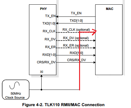
    "the output clock (CLKOUT) of the TLK110 device cannot be used to source the RMII clock to AM335x as doing so would violate the interface timing. Instead, a shared CMOS-level oscillator source would be needed for both MAC and PHY. Please see Figure 4-2 of the TLK datasheet for more details."

    Will it be OK with the below connection?
    If "CLKOUT" of TLK110 couldn't be used then I believe we could use TLK106/TLK105 which
    is little bit low cost than TLK110.

    Regards
    Prad

  • Good catch Prad.

    Further review of the TLK110 documentation reveals that although it does provide a 50MHz clock output, it cannot be used to actually clock the RMII interface, so in the case of TLK110 you would need to use an external 50MHz oscillator as discussed previously.

    I have an email in to the TLK team to verify this...but for now I think it safe to assume that the external oscillator is required for TLK110.

  • Prad,

    I have received verification from the TLK team that the TLK110 clock-out is not intended to be used as the RMII interface clock. An external 50MHz oscillator would be required for RMII operation of this PHY.

  • Thank you very much for the confirmation.

  • ASSERTION

    I believe the AM335x is not guaranteed to work with the TLK110.  The hold time on the TXD lines won't be met.

    I'm suspicious that the AM335x might not be guaranteed to work with a lot of RMII interface PHYs.  Micrel's KSZ8021 for instance requires 8ns hold.

    TIMING DETAILS

    The TLK110 timing requirements are easy to understand for the TXD lines.  There is a setup requirement of 1.4ns and a hold time of 2ns.  (I assume I'm understanding the spec correctly.  The way the t3 timing requirement is named, "data hold to X1 rising", a 2ns hold time implies that the signal stop holding before the clock edge.  It is improbable that this is what is meant since the setup time is 1.4ns.  A better hold description would be "X1 rising to data hold".)  See SLLS901D.pdf table 9-23 for TLK110 TXD timing.


    Understanding the TXD spec for the AM335x is a little more complicated.  SPRS717F.pdf Table 5-15 specifies the TXD timing.  The timing is specified as a delay after clock of between 2ns and 13ns.  This means that the data won't be consumable by the PHY until the next clock.  It also means that the setup and hold time being provided by the AM335x is 7ns setup and 2ns hold.  This assumes perfect clocking with no jitter, and perhaps some other things that keeps TI from spec'ing this as a setup and hold time.  I had to draw the timing out.  If you are trying to thoroughly follow this I suggest drawing out the datavalid vs clock.  Using logic instead of pictures, if the data is valid 2ns after clock, the most the data could have been held from the previous phase is 2ns.  This assumes instantaneous data transitions, and no timing skew between data lines. 

    MITIGATION IDEAS

    Since setup/hold requirements are 1.4ns/2ns, and what is being provided is 7ns/2ns, someone could phase shift the clock by (7-1.4)/2 = 2.8ns.  Assuming a signal speed of 170ps/in, this requires 16" of extra clock lines to center the setup/hold margin.  This probably isn't reasonable.

    SN74LVC1G34 could be used.  At 3.3V Vcc this gives  1.5ns < tpd < 4.1ns.

    Sadly, both of these ideas will make the timing margin for RXD worse.  By the same logic as above, the TLK110 provides setup/hold of 6ns/4ns, while the AM335x requires 4ns/2ns.  Since the TXD has 0ns of design margin, and the RXD has 2ns of design margin, the clock could be phase shifted to one device by 1ns to split the difference.  This would give both TXD and RXD 1ns of timing margin.

    Alternately, the TXD lines could be delayed by 2.8ns.  This wouldn't affect the RXD timing margin.

    I'm uncomfortable with this.  This doesn't feel like a six sigma quality design.


    CONCLUSION

    The AM335x's RMII interface is not appropriate to use with the TLK110.


    COMMENTS / CORRECTIONS?

    Do I have a correct understanding of the timing?

    Is there a recommended TI RMII PHY for use with the AM335x with more robust timing margin?

  • Hi Daniel,

    The appropriateness of a particular PHY/MAC solution has much to do with the nature of the interface on the particular board it is being evaluated for. This is why we strongly recommend that customers take the time to understand the interface and how it relates to the board being evaluated rather than just saying "Yes, x PHY will work:...there are too many variables to makes such a blanket statement. As you have pointed out...there is very little margin on the RMII interface as a whole so even small variables such as prop delay and jitter margin can negatively impact timing to the point of  failures on the interface.

    To touch specifically on the PHYs you mentioned, the TLK110 and the Micrel KSZ80x1RNL, I did a quick timing analysis on these and found them both to be usable (timing-wise) with AM335x at reasonable trace-lengths (I used 5000 mils for all signals in my analysis) as long as certain conditions were met.

    - The Micrel will pass timing in clock out mode only with a minimum 1ns of margin (I'm already assuming 200ps of jitter for all signals). PHY hold margins are grossly violated in clock-in mode, so depending on the desired config of the end-solution, this PHY may not be the best choice for all customers.

    - The TLK110 will also pass in the same scenario with a minimum 750ps of margin (PHY Hold).

    Admittedly, not all systems can be produced with perfect 5000 mil traces and zero inter-bus skew, but this is just an example of what can be accomplished with careful consideration during the layout process.

  • 1.  My analysis was done on paper with the datasheet for the AM335x and TLK110 timing information.  Using equal length traces, I don't see how you can guarantee timing with a 0.75ns hold margin.  Is my paper analysis in error?  Is my paper analysis not sophisticated enough?  Can you explain how you came up with 0.75ns TXD hold margin?  I described my timing analysis method.  Can you describe yours?


    2.  What certain conditions need to be met?  We need to be able to use the part over the whole temperature range.  Restricted temperature range to meet timing wouldn't be acceptable for us.  (Flat out guess that this might have been one of the "certain conditions".)

  • It is not necessary to adjust PCB delays to center the clock in the data valid window.

    The AM335x data sheet publishes output timing parameters as a delay and input timing parameters as setup/hold with respect to a clock edge because that is how synchronous devices operate.

    The timing parameter values published in the data sheet assume worst case operating conditions that include device process variations, voltage variations, and temperature variations.  Therefore, clock source jitter and PCB etch delay are the other major contributors that need to be considered when performing your timing analysis.

    If you have accounted for all of these variables and still have 750ps of margin, you should be okay.

    Regards,
    Paul   

  • Using the spec's from the datasheet, there is 0ps of timing margin.  Accounting for clock jitter and etch delay will show that the design is not stable. 

    I'll state the problem in fewer words.  The AM335x only guarantees 2ns of TXD output "hold time".  The TLk110 requires at least 2ns of TXD input hold time.  This provides 0ps of design margin.  Once accounting for jitter and etch delay, the design isn't guaranteed to work.

    Have I munged up the timing analysis?

  • DK was kind enough to share his calculation used to determine the 750ps margin for the TLK110.

    This is PHY hold margin for TLK110 in clock-in mode. I’m just pointing out that this assumes an external 50MHz oscillator is supplying the clock to both MAC and PHY. All signals are 5000mils in this example and I’m setting the minimum prop delay @ 150 ps/inch.

    (MAC_DELAY_MIN - PHY_HOLD_MIN + (((TXD0_TRACE_LENGTH + MAC_CLK_LENGTH - PHY_CLK_LENGTH) / 1000) * MIN_PCB_PROPAGATION_DELAY)

    or

    (2 - 2 + (((5000 + 5000 - 5000) / 1000) * 150)) = 750ps

  • Thank you everyone.  I understand my error.  I wasn't taking into account the trace propagation delay.  Our design currently only has 1.5" not 5" of traces, but we can fix that next turn.

  • Ok, here I come again.  The above equation is trying to figure out if the TXD waveform from the AM335x will arrive at the TLk110 in time to meet the setup and hold time requirements of the TLK110 (nothing new here). 

    MAC_DELAY_MIN is used to figure out how long the data from the previous phase was held, and by inference, how long the data from the current phase will be held.  The problem is that the above analysis assumes an instantaneous transition between data phases.  The assumption that if data is valid 2ns after the clock, that data from the previous phase was valid 2ns after the clock is invalid.  This assumption is overly optimistic by TR  (This statement is overly pessimistic because data is valid outside of 0.8V to 2.0V.  The whole slew time isn't required to get data valid assuming 10% to 90% was used as thresholds). In reality there is a TR or TF of somewhere between 1 and 5ns that needs to be added to the analysis.  


    I believe the equation should be:

    (MAC_DELAY_MIN - TR_MAX - PHY_HOLD_MIN + (((TXD0_TRACE_LENGTH + MAC_CLK_LENGTH - PHY_CLK_LENGTH) / 1000) * MIN_PCB_PROPAGATION_DELAY)

    or

    (2 - 5 - 2  + (((5000 + 5000 - 5000) / 1000) * 150)) = -4.250ns (worst case TXD timing margin with worst case AM335x delay, worst case PHY hold requirement, and worst case TXD rise time.

    Picking an average rise time (1+5)/2 = 3ns still gives TXD timing margin of -2.25ns.


    If we make the TXD trace (4.25 ns + 1 ns) / 0.15 ns/in = 35in longer, we'll have guaranteed 1ns timing margin over process and temperature.

    Thoughts?


  • The 1-5ns TR is actually defined by the RMII specification...it's not a TI-defined part spec. We characterize our devices to ensure that we meet this requirement and stop at that. It should not be construed as actual characterization data across process/voltage/temp. That said...I do think that it would be useful to attempt to narrow this down (or at least provide a typical value) based on characterization data. Experience with this process node leads me to believe that the true range is much smaller.

    I understand your point when trying to characterize absolute worst-case based on these numbers, but from my perspective I don't see it as necessary given that this is a shared-clock, synchronous, interface and that the TR delta for both the clock and data signals will very likely be within the jitter margin discussed previously. This assumes equivalent loadings and trace-lengths, which I think is a fair assumption. 

    In any case, it would be very valuable to model the interface for your particular implementation prior to committing it to PCB.

  • I usually don't get this detailed with timing.  Based on other things (errata, E2E board) I don't believe the RMII timing was well thought out.  Perhaps this isn't TI's fault.  Maybe RMII isn't well thought out.  Correct or not, I smell blood in the water.  I want to thoroughly check this out.  Consider the possibility that I'm wildly misunderstanding something, and feel free to point it out.

    I don't see how you can say that the 1-5ns TR for RMII TXD isn't TI's spec.  It is Table 5-15 of SPRS717F.pdf.  I feel the need to respect the datasheet.  The fact that 1-5ns come from some other spec, and perhaps TI could have spec'ed it tighter, doesn't allow me to ignore the spec.  For the sake of argument, I'm willing to assume the TR for RMII TXD out of the Sitara will always be 2.5ns exactly with no jitter.  This is consistent with what I've measured on _one_ board.  I'm willing to assume TR is whatever number between 1ns and 5ns because this doesn't affect my assertion that timing is not met for 1ns to 5ns TXD TR.

    ASSERTION

    The assumption that if data is valid 2ns after the clock, that data from the previous phase was valid 2ns after the clock is invalid due to non-zero rise time.

    RAMIFICATIONS

    Ignoring propagation delay there is 0ns timing margin.  (Dan's first post)

    Taking into account propagation delay, as you pointed out, there is 0.75ns timing margin. (DK's reply)

    Taking into account TR decreasing the Sitara held time after clock on TXD, there is 0.75ns - {1 to 5}ns of timing margin.


    CLARIFICATION / RESTATING

    I suspect that you don't understand what I said in my last post.  It isn't that there is a TR delta between the clock and TXD (there is, I'm ignoring it), it is that the guaranteed hold time of TXD after clock is 2ns - TR.

    To restate this again, how long after clock is TXD guaranteed to be held?

    Here is how I came up with TXD held time out of the Sitara number: (snip from previous post)

    MAC_DELAY_MIN is used to figure out how long the data from the previous phase was held, and by inference, how long the data from the current phase will be held.  The problem is that the above analysis assumes an instantaneous transition between data phases.  The assumption that if data is valid 2ns after the clock, that data from the previous phase was valid 2ns after the clock is invalid.  This assumption is overly optimistic by TR  (This statement is overly pessimistic because data is valid outside of 0.8V to 2.0V.)

  • The RMII specification assumes an external 50MHz RMII reference clock is sourced to the MAC and PHY, where they both receive the clock transition at approximately the same time.  After the specification was released several MACs and PHYs were designed to source the RMII reference clock, but this operation is not defined in the RMII specification.

    The assumption stated above about the MAC and PHY receiving the clock transition at the same time is not going to be the case if you use a reference clock sourced by the MAC or PHY.  In this case, the difference in time also needs to be considered when performing timing analysis.

    The RMII specification also defines timing measurements to be referenced from the RMII reference clock crossing a voltage of 1.4 volts to the IO signals being valid at 0.8 or 2.0 volts.

    Therefore, the RMII specification defines the hold time as the minimum time the data must be held below 0.8 volts or above 2.0 volts after the RMII reference clock crosses 1.4 volts at the device terminals.  

    Every AM335x RMII timing parameter published in the data sheet matches the exact values defined in revision 1.2 of the RMII specification except the output delays which are not explicitly defined in the specification.  The following assumption was made when determining valid output delay values.

    Min output delay of 2ns meets the PHY hold time requirement of 2ns while sourcing the clock to the PHY with a worst case output load of 3pf .  Max output delay of 13ns meets the PHY setup time requirement of 4ns with enough margin to provide 2.999ns of round trip PCB etch delay (about 8.8 inches each direction) while receiving the clock from the PHY or external clock source with a worst case output load of 25pf.

    Since AM335x is not able to source the RMII reference clock, it is not possible for AM335x to violate a 2ns hold time since the minimum delay from the clock crossing 1.4 volts to the data beginning to change is 2ns with a minimum load of 3pf. Any PCB delays or loading greater than 3pf on the IO signal will slow the slew rate which will only add to this minimum delay.

    Early in this thread you mentioned a PHY that requires a 8ns hold time.  This PHY clearly violates the 2ns hold time defined in the RMII specification. 

    Regards,
    Paul

  • That is a huge chunk of useful, relevant, dense information.  It is beautiful.  Thank you.

    DISAGREEMENT STATEMENT

    I disagree with your statement (diffs bold):

    "it is not possible for AM335x to violate a 2ns hold time since the minimum delay from the clock crossing 1.4 volts to the data beginning to change is 2ns with a minimum load of 3pf"

    I believe this to be true:

    "It is possible for the AM335x to violate a 2ns hold time since the minimum delay from the clock crossing 1.4 volts to the data being valid is 2ns with a minimum load of 3pf"

    DISAGREEMENT DISSECTION

    I believe these are the critical features of the timing diagram, some of which we disagree on:

    1.  Timing #1 is the delay from clock high (1.4V) to TXD valid (2.0V).  I think we disagree based on your statement.

    2.  The time from clock high (1.4V) to TXD valid (2.0V) is 2ns or more.  I think we disagree.  Based on your statement, I think you believe that 2ns is when the data change starts, not when it is settled.

    3.  The time the previous data phase is guaranteed to be valid after clock can't be more than 2ns - tr(TXD).  I believe this is the critical disagreement caused by the above disagreements. 

    4.  There is an ambiguity in the table and diagram.  The table has REF_CLK high to TXD[1:0] valid for #1, but #1 is drawn from REF_CLK high to TXD[1:0] middle of transition.  I think that regardless of which is true, my assertion is still correct, but the scale of my assertion changes.

    2ns - tr(TXD) is pessimistic because tr(TXD) is 10% - 90% instead of 0.8V to 2V.  I could more accurately say that TXD timing isn't guaranteed because the data is only held for 2ns - tr(TXD*fudge where fudge is time(0.8V -> 2V)/time(10% vmax -> 90% vmax).  I think this can be ignored for now without changing anything other than the degree to which the design is meeting or failing timing.

    I believe that tr(TXD) is being ignored.  I believe that tr(TXD) can't be ignored as it is the equivalent duration to the hold time requirement. The following statement implies that tr(TXD) is being ignored:

    Min output delay of 2ns meets the PHY hold time requirement of 2ns

    REFERENCE

    I'll paste the timing diagram in question for easy reference:

    I believe the following isn't relevant, but I'll state it in case it can clear up ambiguity or misunderstanding somewhere.

    1.  We are using an external clock that is midway between the AM335x and the PHY (TLk100).

    2.  Our AM335x to PHY distance is 1.5" not 5".  I see how if my assertion is incorrect that this will provide only ~220ps of timing margin.  If my assertion is incorrect, I'll probably length the TXD traces only to be 3" or 4" at the next spin.  If my assertion is correct, timing is guaranteed without using a very long TXD trace.  It isn't clear what we'll do in that case.

    3.  RMII clock valid at 1.4V is interested, but I believe irrelevant to this discussion.  The spec's are from clock valid to some event.  Whether clock valid is at 1.4V or 2V will just cause a data valid phasing delay relative to the clock voltage waveforms assuming the AM335x and the PHY both use the same threshold. 

  • Oops, reference #2 above should read "timing is not guaranteed" instead of "timing is guaranteed".

    I tried posting the image of the relevant timing diagram, but it got stripped.

  • The best explanation I've heard so far is that the hold from the AM3352 and the hold requirement at the TLK110 isn't a requirement to hold data valid, but is actually a timing requirement to the zero or threshold crossing.  This interpretation is consistent with the timing diagram in Figure 5-12 of SPRS717.pdf and Figure 9-23 of SLLS901D.  When I think of data valid, I think 2.0V and 0.8V, not threshold crossing. 

    Perhaps this difference explains how the RMII TXD hold provided by the AM3352 and required by the TLK110 is acceptable.