Part Number: AM3352
The 1st spin of our custom board (based on the BeagleBone Black) used the AM3352 with a single Micron MT41K256M16HA-125 and we've already successfully ported U-Boot/SPL and Linux to that.
The 2nd spin is using the a single Micron MT41K256M16TW-107 as a BoM modification, layout has not been changed.
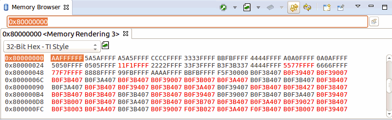
I've been trying to discover the DDR timings for the 2nd spin and unfortunately I'm seeing the "Data Changing Everywhere!" symptom as described here.
I'm attempting to configure the RAM to 6-6-6 800MT/s @ 400MHz. Using the datasheet for MT41K256M16 I came up with the values below:
| Memory datasheet symbol | Memory Datasheet value | unit |
| tCK | 2.5 | ns |
| tRP | 15 | ns |
| tRCD | 15 | ns |
| tWR | 15 | ns |
| tRAS | 37.5 | ns |
| tRC | 52.5 | ns |
| tRRD | 10 | ns |
| tWTR | 10 | ns |
| tXP | 3 | tCK |
| tAOND | 2 | tCK |
| tXSNR | 170 | ns |
| tXSRD | 512 | tCK |
| tRTP | 10 | ns |
| tCKE | 3 | tCK |
| tRFC | 160 | ns |
and from the CAD:
| Parameters | ||
| DDR clock frequency | 400 | MHz |
| PHY_INVERT_CLKOUT | 1 | |
| Trace Length (inches) | ||
| Byte 0 | Byte 1 | |
| DDR_CK trace | 0.823 | 0.823 |
| DDR_DQSx trace | 1.064 | 0.969 |
| Intermediate values (per byte lane) | ||
| WR DQS | 7B | 7D |
| RD DQS | 40 | 40 |
| RD DQS GATE | F6 | F2 |
| Seed values used in CCS code | ||
| DATAx_PHY_RD DQS_SLAVE_RATIO | 40 | |
| DATAx_PHY_FIFO_WE_SLAVE_RATIO | F4 | |
| DATAx_PHY_WR DQS_SLAVE_RATIO | 7C | |
| Register value | ||
| CMDx_PHY_CTRL_SLAVE_RATIO | 100 |
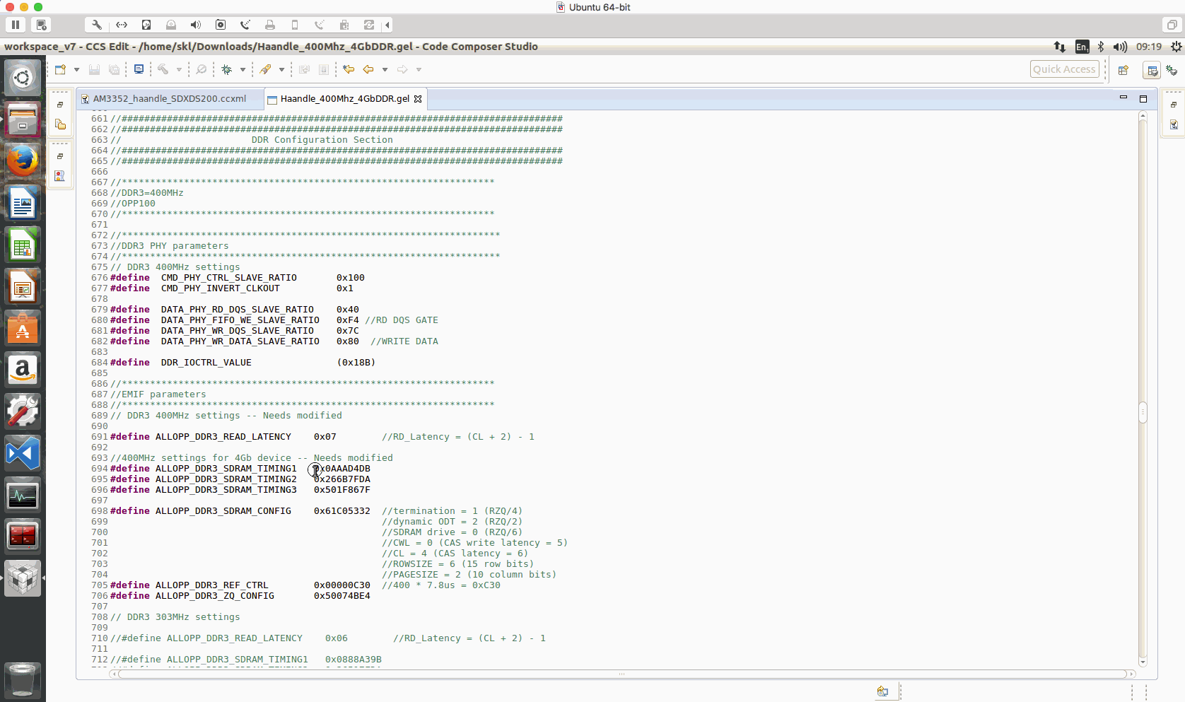
GEL file:
//******************************************************************
//EMIF parameters
//******************************************************************
// DDR3 400MHz settings -- Needs modified

#define ALLOPP_DDR3_READ_LATENCY    0x07        //RD_Latency = (CL + 2) - 1

//400MHz settings for 4Gb device -- Needs modified
#define ALLOPP_DDR3_SDRAM_TIMING1   0x0AAAE51B
#define ALLOPP_DDR3_SDRAM_TIMING2   0x24437FDA
#define ALLOPP_DDR3_SDRAM_TIMING3   0x000003FF

#define ALLOPP_DDR3_SDRAM_CONFIG    0x61C05332  //termination = 1 (RZQ/4)
                                                //dynamic ODT = 2 (RZQ/2)
                                                //SDRAM drive = 0 (RZQ/6)
                                                //CWL = 0 (CAS write latency = 5)
                                                //CL = 4 (CAS latency = 6)
                                                //ROWSIZE = 6 (15 row bits)
                                                //PAGESIZE = 2 (10 column bits)
#define ALLOPP_DDR3_REF_CTRL        0x00000C30  //400 * 7.8us = 0xC30
#define ALLOPP_DDR3_ZQ_CONFIG       0x50074BE4
Summary:
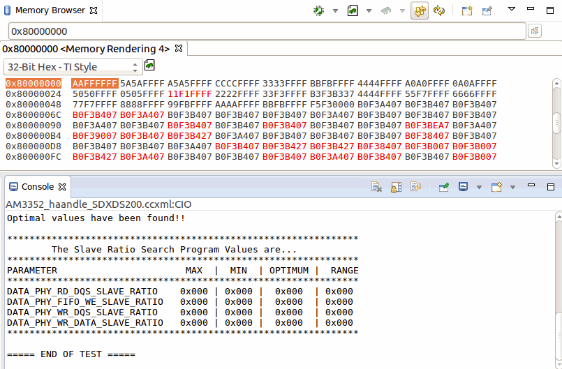
- Software levelling always fails with all zeros
- "Data changing everywhere!" When looking at 0x80000000 with continual refresh
Please advise.
EDIT: Attached datasheet.4Gb_DDR3L.pdf