This thread has been locked.
If you have a related question, please click the "Ask a related question" button in the top right corner. The newly created question will be automatically linked to this question.
Dear Champs,
My customer find the high-byte DQS(UDQS) signal was sent before low-byte DQS(LDQS) and thus there was data missing occurred in high-byte.
Is there any way to control UDQS output time to same as LDQS output time?
My customer changed DDR3 memory in their board and found booting fail occurred.
When I checked their board, I found data missing in the high-byte of memory window in the ccs.
The below is my customer's analysis, and they are afraid that there are too many gaps between UDQS time and LDQS time.
* TI AM3352 sends high-byte DQS (UDQS) before low-byte (LDQS) as waveforms check with UDQS and LDQS,
* But WRITE DQS check with M15F1G1664A(2CS), it seems no consecutive DQS running on AM3352, that means booting failed.
* We suppose that data will be missed to strobe during WRITE cycle, if skew is too wide between UDQS and LDQS sent by chipset.
the below is the measurement data. blue line is UDQS and green line is LDQS.
you can find Time gap of 219.26ps at Rising time and 194.14ps at Falling time.
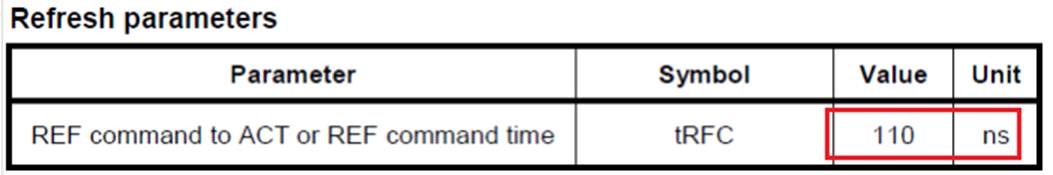
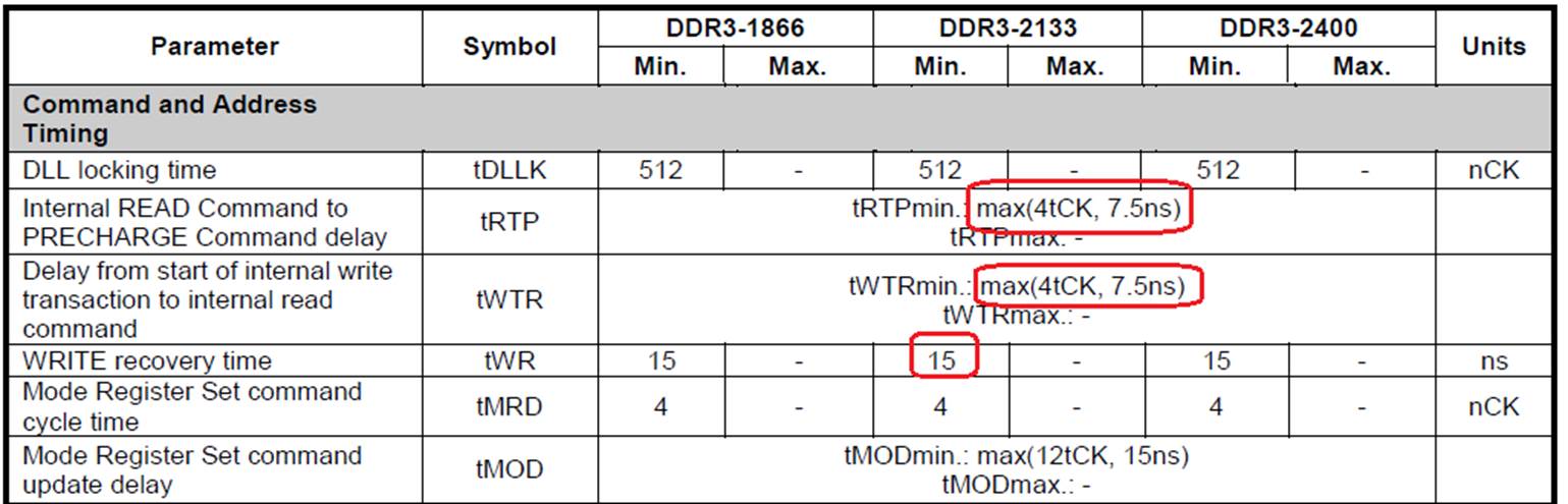
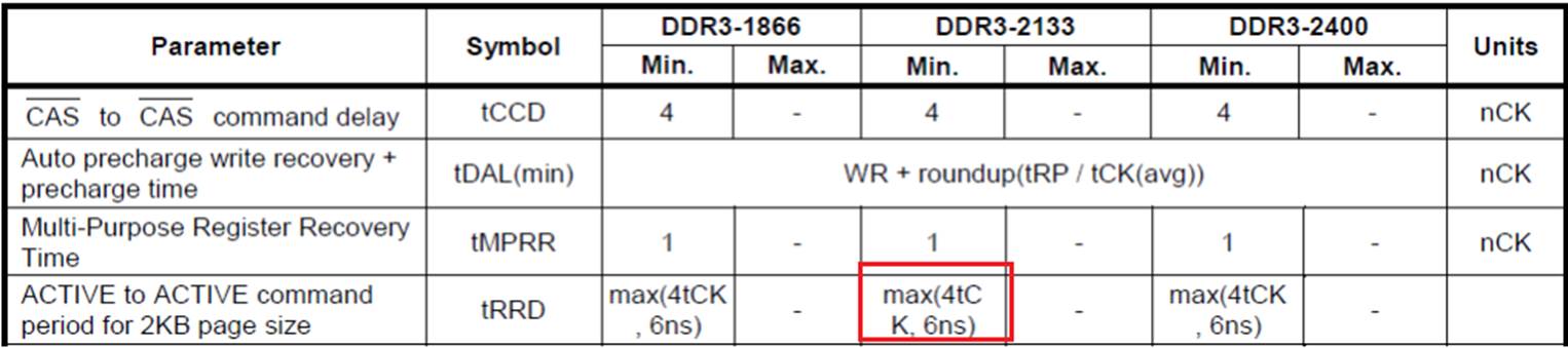
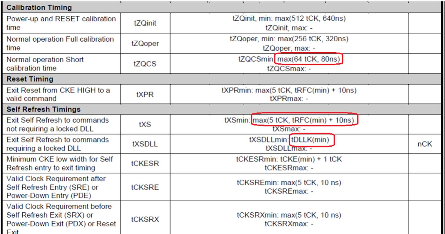
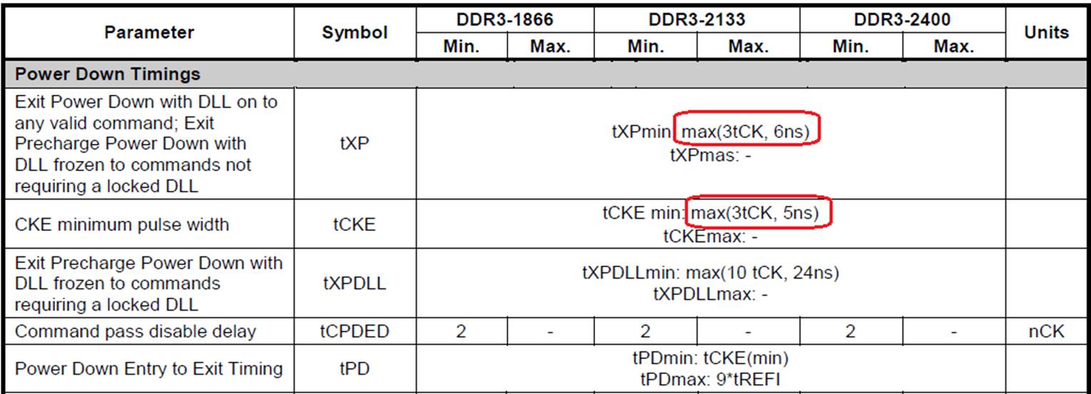
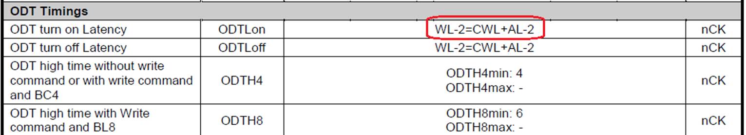
Read tCK(avg): 2.5 ~ 3.3ns, CL=6tCK, Write CWL = 5tCK.
So, if there is a way to control UDQS output time, it would be very helpful.
Thanks and Best Regards,
SI.
Have you gone through the steps for software leveling found here: http://processors.wiki.ti.com/index.php/AM335x_DDR_PHY_register_configuration_for_DDR3_using_Software_Leveling
If your customer has 2 devices in T-topology, they should only have to fill out the Ratio Seed spreadsheet. Ensure that they use a INVERT_CLKOUT setting =1
Regards,
james
Hi James,
As I said, it seemed high-bytes was missed. when I run software leveling as you suggested, I could not find any valid information and all values were 0 as you see in below.
As I said customer has 1 x 16bit DDR memory and CK_length > DQS length, so I used INVERT_CLKOUT setting = 0.
I'm afraid software leveling was not worked properly because high-bytes were missed in the DDR.
When I write '0x5A5A' in the memory window of CCS, I found other 3 following bytes were changed in below.
So, if there is anyway to meet UDQS(highbytes) timing to LDQS(highbytes) before software leveling, it would be very helpful to debug this issue.
The below is the result of software leveling.
~~~~~~~~~~
[CortxA8]
Enter the PHY_INVERT_CLKOUT value (0 or 1) from the spreadsheet
0
Enter the Seed RD_DQS_SLAVE_RATIO Value in Hex to search the RD DQS Ratio Window
40
Enter the Seed FIFO_WE_SLAVE_RATIO Value in Hex to search the RD DQS Gate Window
82
Enter the Seed WR_DQS_SLAVE_RATIO Write DQS Ratio Value in Hex to search the Write DQS Ratio Window
A
***************************************************************
The Slave Ratio Search Program Values are...
***************************************************************
PARAMETER MAX | MIN | OPTIMUM | RANGE
***************************************************************
DATA_PHY_RD_DQS_SLAVE_RATIO 0x000 | 0x000 | 0x000 | 0x000
DATA_PHY_FIFO_WE_SLAVE_RATIO 0x000 | 0x000 | 0x000 | 0x000
DATA_PHY_WR_DQS_SLAVE_RATIO 0x000 | 0x000 | 0x000 | 0x000
DATA_PHY_WR_DATA_SLAVE_RATIO 0x000 | 0x000 | 0x000 | 0x000
***************************************************************
rd_dqs_range = 0
fifo_we_range = 0
wr_dqs_range = 0
wr_data_range = 0
Optimal values have been found!!
***************************************************************
The Slave Ratio Search Program Values are...
***************************************************************
PARAMETER MAX | MIN | OPTIMUM | RANGE
***************************************************************
DATA_PHY_RD_DQS_SLAVE_RATIO 0x000 | 0x000 | 0x000 | 0x000
DATA_PHY_FIFO_WE_SLAVE_RATIO 0x000 | 0x000 | 0x000 | 0x000
DATA_PHY_WR_DQS_SLAVE_RATIO 0x000 | 0x000 | 0x000 | 0x000
DATA_PHY_WR_DATA_SLAVE_RATIO 0x000 | 0x000 | 0x000 | 0x000
***************************************************************
===== END OF TEST =====
Thanks and Best Regards,
SI.
Please find attached file in below.
I modified starter kit GEL file.
RatioSeed_AM335x_boards_ss.xls
RatioSeed_AM335x_boards_ss.pdf
Thanks and Best Regards,
SI.
Can you try changing the following lines below and test again:
#define CMD_PHY_CTRL_SLAVE_RATIO 0x100
#define CMD_PHY_INVERT_CLKOUT 0x1
#define DATA_PHY_RD_DQS_SLAVE_RATIO 0x40
#define DATA_PHY_FIFO_WE_SLAVE_RATIO 0x102 //RD DQS GATE
#define DATA_PHY_WR_DQS_SLAVE_RATIO 0x8A
#define DATA_PHY_WR_DATA_SLAVE_RATIO 0xCA //WRITE DATA
Regards,
James
Hi James,
I changed GEL file as you recommended, but still found same result in below.
[CortxA8]
Enter the PHY_INVERT_CLKOUT value (0 or 1) from the spreadsheet
0
Enter the Seed RD_DQS_SLAVE_RATIO Value in Hex to search the RD DQS Ratio Window
40
Enter the Seed FIFO_WE_SLAVE_RATIO Value in Hex to search the RD DQS Gate Window
82
Enter the Seed WR_DQS_SLAVE_RATIO Write DQS Ratio Value in Hex to search the Write DQS Ratio Window
A
***************************************************************
The Slave Ratio Search Program Values are...
***************************************************************
PARAMETER MAX | MIN | OPTIMUM | RANGE
***************************************************************
DATA_PHY_RD_DQS_SLAVE_RATIO 0x000 | 0x000 | 0x000 | 0x000
DATA_PHY_FIFO_WE_SLAVE_RATIO 0x000 | 0x000 | 0x000 | 0x000
DATA_PHY_WR_DQS_SLAVE_RATIO 0x000 | 0x000 | 0x000 | 0x000
DATA_PHY_WR_DATA_SLAVE_RATIO 0x000 | 0x000 | 0x000 | 0x000
***************************************************************
rd_dqs_range = 0
fifo_we_range = 0
wr_dqs_range = 0
wr_data_range = 0
Optimal values have been found!!
***************************************************************
The Slave Ratio Search Program Values are...
***************************************************************
PARAMETER MAX | MIN | OPTIMUM | RANGE
***************************************************************
DATA_PHY_RD_DQS_SLAVE_RATIO 0x000 | 0x000 | 0x000 | 0x000
DATA_PHY_FIFO_WE_SLAVE_RATIO 0x000 | 0x000 | 0x000 | 0x000
DATA_PHY_WR_DQS_SLAVE_RATIO 0x000 | 0x000 | 0x000 | 0x000
DATA_PHY_WR_DATA_SLAVE_RATIO 0x000 | 0x000 | 0x000 | 0x000
***************************************************************
===== END OF TEST =====
I changed GEL file in below.
//*******************************************************************
//DDR3 PHY parameters
//*******************************************************************
//#define CMD_PHY_CTRL_SLAVE_RATIO 0x40
//#define CMD_PHY_INVERT_CLKOUT 0x1
#define CMD_PHY_CTRL_SLAVE_RATIO 0x100
#define CMD_PHY_INVERT_CLKOUT 0x1
//#define DATA_PHY_RD_DQS_SLAVE_RATIO 0x3B
//#define DATA_PHY_FIFO_WE_SLAVE_RATIO 0x100 //RD DQS GATE
//#define DATA_PHY_WR_DQS_SLAVE_RATIO 0x85
//#define DATA_PHY_WR_DATA_SLAVE_RATIO 0xC1 //WRITE DATA
#define DATA_PHY_RD_DQS_SLAVE_RATIO 0x40
#define DATA_PHY_FIFO_WE_SLAVE_RATIO 0x102 //RD DQS GATE
#define DATA_PHY_WR_DQS_SLAVE_RATIO 0x8A
#define DATA_PHY_WR_DATA_SLAVE_RATIO 0xCA //WRITE DATA
#define DDR_IOCTRL_VALUE (0x18B)
Thanks and Best Regards,
SI.
Hi James,
Any update on this?
Could you please suggest new values to test?
Thanks and Best Regards,
SI.
SI, your DQS signals are different lengths, so it makes sense that the the controller will launch them at slightly different times. Can you send the full GEL file you are using with the changes i suggested above? Also, were all of the layout guidelines followed in the AM335x datasheet, especially for trace length skew? Do you have a trace length report?
Regards,
James
Hi James,
I attached my full GEL file in below.
And also, I would like to check EMIF values and I got confirms it as below from ESMT. Could you please check if below values are right?
Thanks and Best Regards,
SI.
SI, your GEL looks correct based on the datasheet you sent. So with that GEL file, do you still see the errors as you described above? If so, can you also try with the same GEL, but change READ_LATENCY = 0x08.
If you still have problems, then you may have a hardware issue. Can you send the trace length report for the DDR signals? Can you confirm all the design guidelines in the datasheet were followed?
Regards,
James
Hi James,
Unfortunately it was not worked with READ_LATENCY = 0x08 with same situation.
I'm afraid I can not get trace length report although I have requested it, and my customer started to check other device now.
So, I would like to close this.
Actually this is same HW and PCB they have used with Samsung DDR memory. they just changed DDR memory with pin-to-pin device.
So, I think there is no issue in HW related with AM3352, and other DDR memory works well.
Anyway, I have a question.
For ESMT DDR memory failed to work with AM3352, same ESMT DDR memory works well with other devices - processor and FPGA.
Do you think it is reasonable to guess one of reason is because there are HW leveling functions in other device whereas there is no HW leveling in AM3352?
Thanks and Best Regards,
SI.