
- Ask a related questionWhat is a related question?A related question is a question created from another question. When the related question is created, it will be automatically linked to the original question.
This thread has been locked.
If you have a related question, please click the "Ask a related question" button in the top right corner. The newly created question will be automatically linked to this question.
Hi Expert
We got trouble with running DDR3 at clock 400MHz in our DUT that sometimes the system crashed at 303MHz.
We tried to modify the DDR time parameter with the EMIF configuration Tool and still did not work well.
We need your help to check the attached file which we might have the wrong setting or do you have any other common to solve this issue.
Thanks
Daniel
AM335x_EMIF_Configuration_Tool_v3_V73CBG04808RDJ11_shannon.xlsx
#define V73CBG04808RDJ11_CLK	303
#define V73CBG04808RDJ11_EMIF_READ_LATENCY	0x00100208
#define V73CBG04808RDJ11_EMIF_TIM1			0x888A39B
#define V73CBG04808RDJ11_EMIF_TIM2			0x246D7FDA
#define V73CBG04808RDJ11_EMIF_TIM3			0x50FFE6AF
#define V73CBG04808RDJ11_EMIF_SDCFG			0x61A053B2
#define V73CBG04808RDJ11_EMIF_SDREF			0x0000093B
#define V73CBG04808RDJ11_ZQ_CFG				0x50074BE1
#define V73CBG04808RDJ11_RATIO				0x100
#define V73CBG04808RDJ11_INVERT_CLKOUT		0x1
#define V73CBG04808RDJ11_RD_DQS				0x3C
#define V73CBG04808RDJ11_WR_DQS				0xC4
#define V73CBG04808RDJ11_PHY_FIFO_WE		0x118
#define V73CBG04808RDJ11_PHY_WR_DATA		0xFB
#define V73CBG04808RDJ11_IOCTRL_VALUE		0x0000018B

static const struct ddr_data ddr3_pg5902b_data = {
	.datardsratio0 = V73CBG04808RDJ11_RD_DQS,
	.datawdsratio0 = V73CBG04808RDJ11_WR_DQS,
	.datafwsratio0 = V73CBG04808RDJ11_PHY_FIFO_WE,
	.datawrsratio0 = V73CBG04808RDJ11_PHY_WR_DATA,
};

static const struct cmd_control ddr3_pg5902b_cmd_ctrl_data = {
	.cmd0csratio = V73CBG04808RDJ11_RATIO,
	.cmd0iclkout = V73CBG04808RDJ11_INVERT_CLKOUT,

	.cmd1csratio = V73CBG04808RDJ11_RATIO,
	.cmd1iclkout = V73CBG04808RDJ11_INVERT_CLKOUT,

	.cmd2csratio = V73CBG04808RDJ11_RATIO,
	.cmd2iclkout = V73CBG04808RDJ11_INVERT_CLKOUT,
};

static struct emif_regs ddr3_pg5902b_emif_reg_data = {
	.sdram_config = V73CBG04808RDJ11_EMIF_SDCFG,
	.ref_ctrl = V73CBG04808RDJ11_EMIF_SDREF,
	.sdram_tim1 = V73CBG04808RDJ11_EMIF_TIM1,
	.sdram_tim2 = V73CBG04808RDJ11_EMIF_TIM2,
	.sdram_tim3 = V73CBG04808RDJ11_EMIF_TIM3,
	.zq_config = V73CBG04808RDJ11_ZQ_CFG,
	.emif_ddr_phy_ctlr_1 = V73CBG04808RDJ11_EMIF_READ_LATENCY,
};

const struct dpll_params dpll_ddr_pg5902b = {
		V73CBG04808RDJ11_CLK, OSC-1, 1, -1, -1, -1, -1};

const struct dpll_params *get_dpll_ddr_params(void)
{
	return &dpll_ddr_pg5902b;
}

const struct ctrl_ioregs ioregs_pg5902b = {
	.cm0ioctl		= V73CBG04808RDJ11_IOCTRL_VALUE,
	.cm1ioctl		= V73CBG04808RDJ11_IOCTRL_VALUE,
	.cm2ioctl		= V73CBG04808RDJ11_IOCTRL_VALUE,
	.dt0ioctl		= V73CBG04808RDJ11_IOCTRL_VALUE,
	.dt1ioctl		= V73CBG04808RDJ11_IOCTRL_VALUE,
};

void sdram_init(void)
{
	config_ddr(V73CBG04808RDJ11_CLK, &ioregs_pg5902b, &ddr3_pg5902b_data,
		   &ddr3_pg5902b_cmd_ctrl_data, &ddr3_pg5902b_emif_reg_data, 0);
}login as: root root@10.0.50.100's password: # cd /jffs2/ # date && ./memtester 900M Thu Jul 14 07:45:55 UTC 2022 memtester version 4.3.0 (32-bit) Copyright (C) 2001-2012 Charles Cazabon. Licensed under the GNU General Public License version 2 (only). pagesize is 4096 pagesizemask is 0xfffff000 want 900MB (943718400 bytes) got 900MB (943718400 bytes), trying mlock ...locked. Loop 1: Stuck Address : testing 11FAILURE: possible bad address line at offset 0x0f586000. Skipping to next test... Random Value : ok Compare XOR : ok Compare SUB : ok Compare MUL : ok Compare DIV : ok Compare OR : ok Compare AND : ok Sequential Increment: ok Solid Bits : testing 3FAILURE: 0xff00ff00 != 0x00000000 at offset 0x03ee6010. FAILURE: 0x00ff00ff != 0xffffffff at offset 0x03ee6014. FAILURE: 0xff00ff00 != 0x00000000 at offset 0x03ee6018. Block Sequential : setting 0
AM335x DDR3 Software Leveling -- Version: Beta 3.0
                              -- Copyright: Texas Instruments China Local Team
 *************************** Program Start********************************

Please input the AM335x EMIF Timing Configuration:
-- AM335x Default EMIF Timing configuration (for StarterKit EVM) --
DDR3_EMIF_SDRAM_TIM_1 : 0x0888A39B
DDR3_EMIF_SDRAM_TIM_2 : 0x26337FDA
DDR3_EMIF_SDRAM_TIM_3 : 0x501F830F
DDR3_EMIF_SDRAM_CONFIG : 0x61C04AB2

Your choice:  1. Use the default one; 2. Input your own one.
Please Choose The DDR3 Frequency:  1. 303MHz; 2. 400MHz.
DDR3 Frequency is Set at 303MHz!

Please input your DDR3_EMIF_SDRAM_TIM_1 conifguration (in Hex) :
0888A39B
Please input your DDR3_EMIF_SDRAM_TIM_2 conifguration (in Hex) :
246D7FDA
Please input your DDR3_EMIF_SDRAM_TIM_3 conifguration (in Hex) :
50FFE6AF
Please input your DDR3_EMIF_SDRAM_CONFIG conifguration (in Hex) :
61A053B2
Your input EMIF Timing configuration --
DDR3_EMIF_SDRAM_TIM_1 :         0x888A39B
DDR3_EMIF_SDRAM_TIM_2 :         0x246D7FDA
DDR3_EMIF_SDRAM_TIM_3 :         0x50FFE6AF
DDR3_EMIF_SDRAM_CONFIG :        0x61A053B2

Please Enter the PHY_INVERT_CLKOUT value (0 or 1) from the spreadsheet :
1
Please Enter the Seed RD_DQS_SLAVE_RATIO Value in Hex to search the RD DQS Ratio Window :
40
Please Enter the Seed FIFO_WE_SLAVE_RATIO Value in Hex to search the RD DQS Gate Window :
10E
Please Enter the Seed WR_DQS_SLAVE_RATIO Write DQS Ratio Value in Hex to search the Write DQS Ratio Window :
80
Please Enter the Seed PHY_CTRL_SLAVE_RATIO Value in Hex :
100
The ratio seeds for the DDR3 Software Leveling :
invert_clkout =         0x1
RD_DQS_RATIO_VAL =      0x40
FIFO_WE_SLAVE_RATIO =   0x10E
WR_DQS_SLAVE_RATIO =    0x80
PHY_CTRL_SLAVE_RATIO =  0x100

        The Slave Ratio Search Program Values are...
***************************************************************
DATA_PHY_RD_DQS_SLAVE_RATIO is :0x3C
DATA_PHY_FIFO_WE_SLAVE_RATIO is : 0x11C
DATA_PHY_WR_DQS_SLAVE_RATIO is : 0x85
DATA_PHY_WR_DATA_SLAVE_RATIO is : 0xBB
***************************************************************
rd_dqs_range = 60
fifo_we_range = 284
wr_dqs_range = 133
wr_data_range = 187

Optimal values not reached, rerunning program with new values...

        The Slave Ratio Search Program Values are...
***************************************************************
DATA_PHY_RD_DQS_SLAVE_RATIO is :0x3C
DATA_PHY_FIFO_WE_SLAVE_RATIO is : 0x118
DATA_PHY_WR_DQS_SLAVE_RATIO is : 0x88
DATA_PHY_WR_DATA_SLAVE_RATIO is : 0xBF
***************************************************************
rd_dqs_range = 0
fifo_we_range = 4
wr_dqs_range = 3
wr_data_range = 4

Optimal values not reached, rerunning program with new values...

        The Slave Ratio Search Program Values are...
***************************************************************
DATA_PHY_RD_DQS_SLAVE_RATIO is :0x3C
DATA_PHY_FIFO_WE_SLAVE_RATIO is : 0x118
DATA_PHY_WR_DQS_SLAVE_RATIO is : 0x8C
DATA_PHY_WR_DATA_SLAVE_RATIO is : 0xC4
***************************************************************
rd_dqs_range = 0
fifo_we_range = 0
wr_dqs_range = 4
wr_data_range = 5

Optimal values not reached, rerunning program with new values...

        The Slave Ratio Search Program Values are...
***************************************************************
DATA_PHY_RD_DQS_SLAVE_RATIO is :0x3C
DATA_PHY_FIFO_WE_SLAVE_RATIO is : 0x117
DATA_PHY_WR_DQS_SLAVE_RATIO is : 0x90
DATA_PHY_WR_DATA_SLAVE_RATIO is : 0xC6
***************************************************************
rd_dqs_range = 0
fifo_we_range = 1
wr_dqs_range = 4
wr_data_range = 2

Optimal values not reached, rerunning program with new values...

        The Slave Ratio Search Program Values are...
***************************************************************
DATA_PHY_RD_DQS_SLAVE_RATIO is :0x3C
DATA_PHY_FIFO_WE_SLAVE_RATIO is : 0x117
DATA_PHY_WR_DQS_SLAVE_RATIO is : 0x94
DATA_PHY_WR_DATA_SLAVE_RATIO is : 0xCB
***************************************************************
rd_dqs_range = 0
fifo_we_range = 0
wr_dqs_range = 4
wr_data_range = 5

Optimal values not reached, rerunning program with new values...

        The Slave Ratio Search Program Values are...
***************************************************************
DATA_PHY_RD_DQS_SLAVE_RATIO is :0x3C
DATA_PHY_FIFO_WE_SLAVE_RATIO is : 0x117
DATA_PHY_WR_DQS_SLAVE_RATIO is : 0x98
DATA_PHY_WR_DATA_SLAVE_RATIO is : 0xCF
***************************************************************
rd_dqs_range = 0
fifo_we_range = 0
wr_dqs_range = 4
wr_data_range = 4

Optimal values not reached, rerunning program with new values...

        The Slave Ratio Search Program Values are...
***************************************************************
DATA_PHY_RD_DQS_SLAVE_RATIO is :0x3C
DATA_PHY_FIFO_WE_SLAVE_RATIO is : 0x118
DATA_PHY_WR_DQS_SLAVE_RATIO is : 0x9D
DATA_PHY_WR_DATA_SLAVE_RATIO is : 0xD3
***************************************************************
rd_dqs_range = 0
fifo_we_range = 1
wr_dqs_range = 5
wr_data_range = 4

Optimal values not reached, rerunning program with new values...

        The Slave Ratio Search Program Values are...
***************************************************************
DATA_PHY_RD_DQS_SLAVE_RATIO is :0x3C
DATA_PHY_FIFO_WE_SLAVE_RATIO is : 0x119
DATA_PHY_WR_DQS_SLAVE_RATIO is : 0xA2
DATA_PHY_WR_DATA_SLAVE_RATIO is : 0xD8
***************************************************************
rd_dqs_range = 0
fifo_we_range = 1
wr_dqs_range = 5
wr_data_range = 5

Optimal values not reached, rerunning program with new values...

        The Slave Ratio Search Program Values are...
***************************************************************
DATA_PHY_RD_DQS_SLAVE_RATIO is :0x3C
DATA_PHY_FIFO_WE_SLAVE_RATIO is : 0x11A
DATA_PHY_WR_DQS_SLAVE_RATIO is : 0xA8
DATA_PHY_WR_DATA_SLAVE_RATIO is : 0xDD
***************************************************************
rd_dqs_range = 0
fifo_we_range = 1
wr_dqs_range = 6
wr_data_range = 5

Optimal values not reached, rerunning program with new values...

        The Slave Ratio Search Program Values are...
***************************************************************
DATA_PHY_RD_DQS_SLAVE_RATIO is :0x3C
DATA_PHY_FIFO_WE_SLAVE_RATIO is : 0x11A
DATA_PHY_WR_DQS_SLAVE_RATIO is : 0xAD
DATA_PHY_WR_DATA_SLAVE_RATIO is : 0xE3
***************************************************************
rd_dqs_range = 0
fifo_we_range = 0
wr_dqs_range = 5
wr_data_range = 6

Optimal values not reached, rerunning program with new values...

        The Slave Ratio Search Program Values are...
***************************************************************
DATA_PHY_RD_DQS_SLAVE_RATIO is :0x3C
DATA_PHY_FIFO_WE_SLAVE_RATIO is : 0x11A
DATA_PHY_WR_DQS_SLAVE_RATIO is : 0xB0
DATA_PHY_WR_DATA_SLAVE_RATIO is : 0xE8
***************************************************************
rd_dqs_range = 0
fifo_we_range = 0
wr_dqs_range = 3
wr_data_range = 5

Optimal values not reached, rerunning program with new values...

        The Slave Ratio Search Program Values are...
***************************************************************
DATA_PHY_RD_DQS_SLAVE_RATIO is :0x3C
DATA_PHY_FIFO_WE_SLAVE_RATIO is : 0x117
DATA_PHY_WR_DQS_SLAVE_RATIO is : 0xB4
DATA_PHY_WR_DATA_SLAVE_RATIO is : 0xEC
***************************************************************
rd_dqs_range = 0
fifo_we_range = 3
wr_dqs_range = 4
wr_data_range = 4

Optimal values not reached, rerunning program with new values...

        The Slave Ratio Search Program Values are...
***************************************************************
DATA_PHY_RD_DQS_SLAVE_RATIO is :0x3C
DATA_PHY_FIFO_WE_SLAVE_RATIO is : 0x118
DATA_PHY_WR_DQS_SLAVE_RATIO is : 0xB8
DATA_PHY_WR_DATA_SLAVE_RATIO is : 0xEE
***************************************************************
rd_dqs_range = 0
fifo_we_range = 1
wr_dqs_range = 4
wr_data_range = 2

Optimal values not reached, rerunning program with new values...

        The Slave Ratio Search Program Values are...
***************************************************************
DATA_PHY_RD_DQS_SLAVE_RATIO is :0x3C
DATA_PHY_FIFO_WE_SLAVE_RATIO is : 0x117
DATA_PHY_WR_DQS_SLAVE_RATIO is : 0xBD
DATA_PHY_WR_DATA_SLAVE_RATIO is : 0xF2
***************************************************************
rd_dqs_range = 0
fifo_we_range = 1
wr_dqs_range = 5
wr_data_range = 4

Optimal values not reached, rerunning program with new values...

        The Slave Ratio Search Program Values are...
***************************************************************
DATA_PHY_RD_DQS_SLAVE_RATIO is :0x3C
DATA_PHY_FIFO_WE_SLAVE_RATIO is : 0x117
DATA_PHY_WR_DQS_SLAVE_RATIO is : 0xC1
DATA_PHY_WR_DATA_SLAVE_RATIO is : 0xF9
***************************************************************
rd_dqs_range = 0
fifo_we_range = 0
wr_dqs_range = 4
wr_data_range = 7

Optimal values not reached, rerunning program with new values...

        The Slave Ratio Search Program Values are...
***************************************************************
DATA_PHY_RD_DQS_SLAVE_RATIO is :0x3C
DATA_PHY_FIFO_WE_SLAVE_RATIO is : 0x118
DATA_PHY_WR_DQS_SLAVE_RATIO is : 0xC4
DATA_PHY_WR_DATA_SLAVE_RATIO is : 0xFB
***************************************************************
rd_dqs_range = 0
fifo_we_range = 1
wr_dqs_range = 3
wr_data_range = 2

Optimal values have been found!!

***************************************************************
DATA_PHY_RD_DQS_SLAVE_RATIO is :0x3C
DATA_PHY_FIFO_WE_SLAVE_RATIO is : 0x118
DATA_PHY_WR_DQS_SLAVE_RATIO is : 0xC4
DATA_PHY_WR_DATA_SLAVE_RATIO is : 0xFB
***************************************************************

===== END OF TEST =====
DDR3 software leveling done!
AM335x DDR3 Software Leveling -- Version: Beta 3.0
                              -- Copyright: Texas Instruments China Local Team
 *************************** Program Start********************************

Please input the AM335x EMIF Timing Configuration:
-- AM335x Default EMIF Timing configuration (for StarterKit EVM) --
DDR3_EMIF_SDRAM_TIM_1 : 0x0888A39B
DDR3_EMIF_SDRAM_TIM_2 : 0x26337FDA
DDR3_EMIF_SDRAM_TIM_3 : 0x501F830F
DDR3_EMIF_SDRAM_CONFIG : 0x61C04AB2

Your choice:  1. Use the default one; 2. Input your own one.
Please Choose The DDR3 Frequency:  1. 303MHz; 2. 400MHz.
DDR3 Frequency is Set at 400MHz!

Please input your DDR3_EMIF_SDRAM_TIM_1 conifguration (in Hex) :
0AAAD4DB
Please input your DDR3_EMIF_SDRAM_TIM_2 conifguration (in Hex) :
248F7FDA
Please input your DDR3_EMIF_SDRAM_TIM_3 conifguration (in Hex) :
50FFE8BF
Please input your DDR3_EMIF_SDRAM_CONFIG conifguration (in Hex) :
61A053B2
Your input EMIF Timing configuration --
DDR3_EMIF_SDRAM_TIM_1 :         0xAAAD4DB
DDR3_EMIF_SDRAM_TIM_2 :         0x248F7FDA
DDR3_EMIF_SDRAM_TIM_3 :         0x50FFE8BF
DDR3_EMIF_SDRAM_CONFIG :        0x61A053B2

Please Enter the PHY_INVERT_CLKOUT value (0 or 1) from the spreadsheet :
1
Please Enter the Seed RD_DQS_SLAVE_RATIO Value in Hex to search the RD DQS Ratio Window :
40
Please Enter the Seed FIFO_WE_SLAVE_RATIO Value in Hex to search the RD DQS Gate Window :
128
Please Enter the Seed WR_DQS_SLAVE_RATIO Write DQS Ratio Value in Hex to search the Write DQS Ratio Window :
80
Please Enter the Seed PHY_CTRL_SLAVE_RATIO Value in Hex :
100
The ratio seeds for the DDR3 Software Leveling :
invert_clkout =         0x1
RD_DQS_RATIO_VAL =      0x40
FIFO_WE_SLAVE_RATIO =   0x128
WR_DQS_SLAVE_RATIO =    0x80
PHY_CTRL_SLAVE_RATIO =  0x100

        The Slave Ratio Search Program Values are...
***************************************************************
DATA_PHY_RD_DQS_SLAVE_RATIO is :0x0
DATA_PHY_FIFO_WE_SLAVE_RATIO is : 0x0
DATA_PHY_WR_DQS_SLAVE_RATIO is : 0x0
DATA_PHY_WR_DATA_SLAVE_RATIO is : 0x0
***************************************************************
rd_dqs_range = 0
fifo_we_range = 0
wr_dqs_range = 0
wr_data_range = 0

Optimal values have been found!!

***************************************************************
DATA_PHY_RD_DQS_SLAVE_RATIO is :0x0
DATA_PHY_FIFO_WE_SLAVE_RATIO is : 0x0
DATA_PHY_WR_DQS_SLAVE_RATIO is : 0x0
DATA_PHY_WR_DATA_SLAVE_RATIO is : 0x0
***************************************************************

===== END OF TEST =====
DDR3 software leveling done!

Can you send the datasheet (or part number if datasheet is available on the web)?
It appears that the timing registers that you input in the the software leveling algorithm does not match what is in your xls. The leveling algorithm shows this:
Please input your DDR3_EMIF_SDRAM_TIM_1 conifguration (in Hex) :
0888A39B
Please input your DDR3_EMIF_SDRAM_TIM_2 conifguration (in Hex) :
246D7FDA
Please input your DDR3_EMIF_SDRAM_TIM_3 conifguration (in Hex) :
50FFE6AF
Please input your DDR3_EMIF_SDRAM_CONFIG conifguration (in Hex) :
61A053B2
Your input EMIF Timing configuration --
DDR3_EMIF_SDRAM_TIM_1 : 0x888A39B
DDR3_EMIF_SDRAM_TIM_2 : 0x246D7FDA
DDR3_EMIF_SDRAM_TIM_3 : 0x50FFE6AF
DDR3_EMIF_SDRAM_CONFIG : 0x61A053B2
but your spreadsheet shows this:
SDRAM_TIM_1 0x4C000018 0x0AAAD4DB
SDRAM_TIM_2 0x4C000020 0x248F7FDA
SDRAM_TIM_3 0x4C000028 0x50FFE8BF
SDRAM_CONFIG 0x4C000008 0x61A053B2
This may be one reason you are getting poor results
Regards,
James
Hi James,
We have done twice with software leveling,
First with 400MHz, according to spreadsheet, I filled,
DDR3_EMIF_SDRAM_TIM_1 : 0xAAAD4DB
DDR3_EMIF_SDRAM_TIM_2 : 0x248F7FDA
DDR3_EMIF_SDRAM_TIM_3 : 0x50FFE8BF
DDR3_EMIF_SDRAM_CONFIG : 0x61A053B2
But it replied 0 at all.
Second time with 303MHz, I changed frequency to 303 in spreadsheet, then filled,
DDR3_EMIF_SDRAM_TIM_1 : 0x888A39B
DDR3_EMIF_SDRAM_TIM_2 : 0x246D7FDA
DDR3_EMIF_SDRAM_TIM_3 : 0x50FFE6AF
DDR3_EMIF_SDRAM_CONFIG : 0x61A053B2
It have found optimal value, but it can't pass memtester and system crashing randomly.
Jimmy
Hi James
7331.DDR3.pdfV73CBG04808RDJJ11I.PDF
Attached files are DDR Datasheet and Schematic
Thanks
Daniel
Hi Daniel, it looks like everything you are showing me is correct so far.
-For the trace length values you have plugged into the tool, is the clock to byte 0 2.22in, and byte 1 61in? Double check that those are not swapped
-Have you followed all the DDR layout guidelines in the AM335x datasheet, especially length matching guidelines?
-at 303MHz, do multiple boards have similar results for the leveling algorithm?
-for the 303MHz case, can you dump the EMIF registers in u-boot. Addresses 0x4c000000-0x4c0000E8
-can you successfully perform single memory write and reads in u-boot?
-do you ever have a problem booting, or do you only see a problem when running memtester?
-for the 303MHz memtester run, it appears that byte1 is faulty. Is this consistent across multiple memtester runs and multiple boards?
Regards,
James
Hi James
1.
I test 3 boards so far, the result as below,
#1
***************************************************************
DATA_PHY_RD_DQS_SLAVE_RATIO is :0x3C
DATA_PHY_FIFO_WE_SLAVE_RATIO is : 0x119
DATA_PHY_WR_DQS_SLAVE_RATIO is : 0xC6
DATA_PHY_WR_DATA_SLAVE_RATIO is : 0xFF
***************************************************************
#3
***************************************************************
DATA_PHY_RD_DQS_SLAVE_RATIO is :0x3C
DATA_PHY_FIFO_WE_SLAVE_RATIO is : 0x11D
DATA_PHY_WR_DQS_SLAVE_RATIO is : 0x8B
DATA_PHY_WR_DATA_SLAVE_RATIO is : 0xC5
***************************************************************
#4
***************************************************************
DATA_PHY_RD_DQS_SLAVE_RATIO is :0x3C
DATA_PHY_FIFO_WE_SLAVE_RATIO is : 0x11C
DATA_PHY_WR_DQS_SLAVE_RATIO is : 0x89
DATA_PHY_WR_DATA_SLAVE_RATIO is : 0xC3
***************************************************************
2.
for the 303MHz case, can you dump the EMIF registers in u-boot. Addresses 0x4c000000-0x4c0000E8
I using board 1 to display register
U-Boot# md 0x4c000000 0x3A
4c000000: 40443403 40000004 61a053b2 00000000 .4D@...@.S.a....
4c000010: 0000093b 0000093b 0888a39b 0888a39b ;...;...........
4c000020: 246d7fda 246d7fda 50ffe6af 50ffe6af ..m$..m$...P...P
4c000030: 00000000 00000000 00000000 00000000 ................
4c000040: 00000000 00000000 00000000 00000000 ................
4c000050: 00000000 00ffffff 8000140a 00021616 ................
4c000060: 00002011 00000000 00000000 00000000 . ..............
4c000070: 00000000 00000000 00000000 00000000 ................
4c000080: 00600242 000568af 00010000 00000000 B.`..h..........
4c000090: 3a43ca80 00000000 00050000 00050000 ..C:............
4c0000a0: 00000000 00000000 00000000 00000000 ................
4c0000b0: 00000000 00000000 00000000 00000000 ................
4c0000c0: 00000000 00000000 50074be1 00000000 .........K.P....
4c0000d0: 00000000 00000000 00000000 00000000 ................
4c0000e0: 00000000 00100208 ........
3.
can you successfully perform single memory write and reads in u-boot?
Sorry, I can’t get the point,
What’s the purpose?
I can load kernel and file system from eMMC to DDR to booting.
4.
-do you ever have a problem booting, or do you only see a problem when running memtester?
Kernel might be crash during booting or finish booting.
5.
-for the 303MHz memtester run, it appears that byte1 is faulty. Is this consistent across multiple memtester runs and multiple boards?
The board 3 and 4 seem have different value when software leveling,
And board 3 and 4 are more difficult to finish kernel booting, usually crash during kernel booting.
Thanks
Daniel
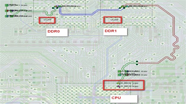
Hi James
For the trace length values you have plugged into the tool, is the clock to byte 0 2.22in, and byte 1 61in?
As the schematic, the DDR U3 connects to the CPU with the net name DQS0. Is it mean that refers to byte0?
And then the other DDR U4 will represent the byte1. Right.
From the below Layout trace figure, we might find that the Byte 0 length is longer than Byte 1.
I have tried to re-calculator the length of the trace, please see the attached file. We might use this value for the EMIF tool.
Have you followed all the DDR layout guidelines in the AM335x datasheet, especially length matching guidelines?
Yes, we have followed the length matching guidelines, please see the attached excel file.
6562.Length.docxPG5902_AM335x_Trace Length Report 20220420.xlsx
Thanks
Daniel
Daniel, thank you for the info
One thing i see in your trace length report is that CK to Addr_ctrl skew is almost 200mil. This should be <25mil based on table 7-66 (A1+A2 skew < 25mil). The skew should be calculated for each segment as shown in the table. I think this may be why you have a little more success as slower frequencies. The excessive skew is severely eating into your timing margin.
Also, the number of vias on the differential CK signals seems excessive (6). This is a critical signal to route, and the vias introduce impedance discontinuities which can lead to poor signal quality. Need to ensure CK and the addr_ctrl signals are routed similarly, with a solid ground reference.
Were any signal integrity board simulations performed on this board?
We can try to get this board functional. I think you will have to stick with 303MHz. It appears the software leveling algorithm is having a hard time converging to optimal values, so i think you may have to experiment manually to see if you can get things functional. Can you try the following experiments
Build you code with the following values, which are the original seed values from the spreadsheet:
#define V73CBG04808RDJ11_RD_DQS 0x40
#define V73CBG04808RDJ11_WR_DQS 0x10E
#define V73CBG04808RDJ11_PHY_FIFO_WE 0x80
#define V73CBG04808RDJ11_PHY_WR_DATA 0xC0
-try to boot and run memtester with this build
-add 0x10 to both PHY_FIFO_WE and PHY_WR_DATA and repeat the experiment of booting and memtester
-continue adding 0x10 and repeat the experiment, until you can't boot anymore. I would expect this to be around when PHY_FIFO_WE is 0xD0 or above
Record the results. The experiments are attempting to find the optimal values for the write path. I think the read path value are ok, based on your algorithm results. Hopefully this will at least get you functional.
Regards,
James
#define V73CBG04808RDJ11_RD_DQS 0x40
#define V73CBG04808RDJ11_WR_DQS 0x10E
#define V73CBG04808RDJ11_PHY_FIFO_WE 0x80
#define V73CBG04808RDJ11_PHY_WR_DATA 0xC0
Hi James,
Are there any typo on the value?
The spreadsheet shows as below in 303M
#define DATA_PHY_RD_DQS_SLAVE_RATIO 0x00000040
#define DATA_PHY_FIFO_WE_SLAVE_RATIO 0x0000010E
#define DATA_PHY_WR_DQS_SLAVE_RATIO 0x00000080
#define DATA_PHY_WR_DATA_SLAVE_RATIO 0x000000C0
Hi James,
I have done below test, it seem that I can't find functional value manually.
#define V73CBG04808RDJ11_RD_DQS 0x00000040
#define V73CBG04808RDJ11_WR_DQS 0x00000080
#define V73CBG04808RDJ11_PHY_FIFO_WE 0x0000010E
#define V73CBG04808RDJ11_PHY_WR_DATA 0x000000C0
Crash during boot
Crash during boot
Crash during boot
#define V73CBG04808RDJ11_RD_DQS 0x00000040
#define V73CBG04808RDJ11_WR_DQS 0x00000080
#define V73CBG04808RDJ11_PHY_FIFO_WE 0x0000011E
#define V73CBG04808RDJ11_PHY_WR_DATA 0x000000D0
Crash during boot
Crash during boot
Crash during boot
#define V73CBG04808RDJ11_RD_DQS 0x00000040
#define V73CBG04808RDJ11_WR_DQS 0x00000080
#define V73CBG04808RDJ11_PHY_FIFO_WE 0x0000012E
#define V73CBG04808RDJ11_PHY_WR_DATA 0x000000E0
Crash during boot
memtester 20M 10 fail and crash
Crash during boot
#define V73CBG04808RDJ11_RD_DQS 0x00000040
#define V73CBG04808RDJ11_WR_DQS 0x00000080
#define V73CBG04808RDJ11_PHY_FIFO_WE 0x0000013E
#define V73CBG04808RDJ11_PHY_WR_DATA 0x000000F0
can't boot
#define V73CBG04808RDJ11_RD_DQS 0x40
#define V73CBG04808RDJ11_WR_DQS 0x10E
#define V73CBG04808RDJ11_PHY_FIFO_WE 0x80
#define V73CBG04808RDJ11_PHY_WR_DATA 0xC0
can't boot
#define V73CBG04808RDJ11_RD_DQS 0x40
#define V73CBG04808RDJ11_WR_DQS 0x10E
#define V73CBG04808RDJ11_PHY_FIFO_WE 0x90
#define V73CBG04808RDJ11_PHY_WR_DATA 0xD0
can't boot
#define V73CBG04808RDJ11_RD_DQS 0x40
#define V73CBG04808RDJ11_WR_DQS 0x10E
#define V73CBG04808RDJ11_PHY_FIFO_WE 0xA0
#define V73CBG04808RDJ11_PHY_WR_DATA 0xE0
can't boot
#define V73CBG04808RDJ11_RD_DQS 0x40
#define V73CBG04808RDJ11_WR_DQS 0x10E
#define V73CBG04808RDJ11_PHY_FIFO_WE 0xB0
#define V73CBG04808RDJ11_PHY_WR_DATA 0xF0
can't boot
#define V73CBG04808RDJ11_RD_DQS 0x40
#define V73CBG04808RDJ11_WR_DQS 0x10E
#define V73CBG04808RDJ11_PHY_FIFO_WE 0xC0
#define V73CBG04808RDJ11_PHY_WR_DATA 0x100
can't boot
#define V73CBG04808RDJ11_RD_DQS 0x40
#define V73CBG04808RDJ11_WR_DQS 0x10E
#define V73CBG04808RDJ11_PHY_FIFO_WE 0xD0
#define V73CBG04808RDJ11_PHY_WR_DATA 0x110
can't boot
Hi James
The attachment is the signal integrity board simulations performed report.
Thanks
Daniel
Jimmy, I'm very sorry, i transposed the parameters that i told you to adjust.
You're original values are this:
#define V73CBG04808RDJ11_RD_DQS 0x3C
#define V73CBG04808RDJ11_WR_DQS 0x80
#define V73CBG04808RDJ11_PHY_FIFO_WE 0x10E
#define V73CBG04808RDJ11_PHY_WR_DATA 0xC0
-try to boot and run memtester with this build
-add 0x10 to both PHY_WR_DQS and PHY_WR_DATA and repeat the experiment of booting and memtester
-continue adding 0x10 and repeat the experiment, until you can't boot anymore. I would expect this to be around when PHY_WR_DQS is 0xD0 or above
I took a look at your report, it seems like you have plenty of margin, I'm not sure why the algorithm isn't converging. Do you have JTAG access to your board. The latest algorithm is downloadable via JTAG and can be found here: https://www.ti.com/lit/pdf/SPRACK4 You are using a u-boot version of the tool which I'm not sure is the latest. Can you try the file in the zip that is in the app note, and use the .out and gel file in there?
Regards,
james
Hi James,
I have finished WR DQS manually,
Unfortunately, the system still unsteady.
#define V73CBG04808RDJ11_RD_DQS 0x3C
#define V73CBG04808RDJ11_WR_DQS 0x80
#define V73CBG04808RDJ11_PHY_FIFO_WE 0x10E
#define V73CBG04808RDJ11_PHY_WR_DATA 0xC0
Crash during boot
memtester 20M 10 fail and crash
Crash during boot
#define V73CBG04808RDJ11_RD_DQS 0x3C
#define V73CBG04808RDJ11_WR_DQS 0x90
#define V73CBG04808RDJ11_PHY_FIFO_WE 0x10E
#define V73CBG04808RDJ11_PHY_WR_DATA 0xD0
Crash during boot
Crash during boot
Crash during boot
#define V73CBG04808RDJ11_RD_DQS 0x3C
#define V73CBG04808RDJ11_WR_DQS 0xA0
#define V73CBG04808RDJ11_PHY_FIFO_WE 0x10E
#define V73CBG04808RDJ11_PHY_WR_DATA 0xE0
Crash during boot
Crash during boot
Crash during boot
#define V73CBG04808RDJ11_RD_DQS 0x3C
#define V73CBG04808RDJ11_WR_DQS 0xB0
#define V73CBG04808RDJ11_PHY_FIFO_WE 0x10E
#define V73CBG04808RDJ11_PHY_WR_DATA 0xF0
memtester 20M 10 fail and crash
Crash during boot
Crash during boot
#define V73CBG04808RDJ11_RD_DQS 0x3C
#define V73CBG04808RDJ11_WR_DQS 0xC0
#define V73CBG04808RDJ11_PHY_FIFO_WE 0x10E
#define V73CBG04808RDJ11_PHY_WR_DATA 0x100
Crash during boot
memtester 20M 10 fail and crash
Crash during boot
#define V73CBG04808RDJ11_RD_DQS 0x3C
#define V73CBG04808RDJ11_WR_DQS 0xD0
#define V73CBG04808RDJ11_PHY_FIFO_WE 0x10E
#define V73CBG04808RDJ11_PHY_WR_DATA 0x110
Crash during boot
Crash during boot
Crash during boot
#define V73CBG04808RDJ11_RD_DQS 0x3C
#define V73CBG04808RDJ11_WR_DQS 0xE0
#define V73CBG04808RDJ11_PHY_FIFO_WE 0x10E
#define V73CBG04808RDJ11_PHY_WR_DATA 0x120
Crash during boot
Crash during boot
Crash during boot
#define V73CBG04808RDJ11_RD_DQS 0x3C
#define V73CBG04808RDJ11_WR_DQS 0xF0
#define V73CBG04808RDJ11_PHY_FIFO_WE 0x10E
#define V73CBG04808RDJ11_PHY_WR_DATA 0x130
memtester 20M 1 fail
Crash during boot
Crash during boot
#define V73CBG04808RDJ11_RD_DQS 0x3C
#define V73CBG04808RDJ11_WR_DQS 0x100
#define V73CBG04808RDJ11_PHY_FIFO_WE 0x10E
#define V73CBG04808RDJ11_PHY_WR_DATA 0x140
can't boot
#define V73CBG04808RDJ11_RD_DQS 0x40
#define V73CBG04808RDJ11_WR_DQS 0x80
#define V73CBG04808RDJ11_PHY_FIFO_WE 0x10E
#define V73CBG04808RDJ11_PHY_WR_DATA 0xC0
memtester 20M 10 fail and crash
Crash during boot
Crash during boot
#define V73CBG04808RDJ11_RD_DQS 0x40
#define V73CBG04808RDJ11_WR_DQS 0x90
#define V73CBG04808RDJ11_PHY_FIFO_WE 0x10E
#define V73CBG04808RDJ11_PHY_WR_DATA 0xD0
memtester 20M 1 fail
Crash during boot
Crash during boot
#define V73CBG04808RDJ11_RD_DQS 0x40
#define V73CBG04808RDJ11_WR_DQS 0xA0
#define V73CBG04808RDJ11_PHY_FIFO_WE 0x10E
#define V73CBG04808RDJ11_PHY_WR_DATA 0xE0
Crash during boot
Crash during boot
Crash during boot
#define V73CBG04808RDJ11_RD_DQS 0x40
#define V73CBG04808RDJ11_WR_DQS 0xB0
#define V73CBG04808RDJ11_PHY_FIFO_WE 0x10E
#define V73CBG04808RDJ11_PHY_WR_DATA 0xF0
Crash during boot
Crash during boot
Crash during boot
#define V73CBG04808RDJ11_RD_DQS 0x40
#define V73CBG04808RDJ11_WR_DQS 0xC0
#define V73CBG04808RDJ11_PHY_FIFO_WE 0x10E
#define V73CBG04808RDJ11_PHY_WR_DATA 0x100
memtester 20M 10 fail and crash
Crash during boot
Crash during boot
#define V73CBG04808RDJ11_RD_DQS 0x40
#define V73CBG04808RDJ11_WR_DQS 0xD0
#define V73CBG04808RDJ11_PHY_FIFO_WE 0x10E
#define V73CBG04808RDJ11_PHY_WR_DATA 0x110
Crash during boot
Crash during boot
memtester 20M 10 fail and crash
#define V73CBG04808RDJ11_RD_DQS 0x40
#define V73CBG04808RDJ11_WR_DQS 0xE0
#define V73CBG04808RDJ11_PHY_FIFO_WE 0x10E
#define V73CBG04808RDJ11_PHY_WR_DATA 0x120
Crash during boot
Crash during boot
Crash during boot
#define V73CBG04808RDJ11_RD_DQS 0x40
#define V73CBG04808RDJ11_WR_DQS 0xF0
#define V73CBG04808RDJ11_PHY_FIFO_WE 0x10E
#define V73CBG04808RDJ11_PHY_WR_DATA 0x130
Crash during boot
Crash during boot
Crash during boot
#define V73CBG04808RDJ11_RD_DQS 0x40
#define V73CBG04808RDJ11_WR_DQS 0x100
#define V73CBG04808RDJ11_PHY_FIFO_WE 0x10E
#define V73CBG04808RDJ11_PHY_WR_DATA 0x140
can't boot
I have got a jTag this morning, and I finished software leveling in CCS today,
The console information of CCS
[CortxA8]
Enter the PHY_INVERT_CLKOUT value (0 or 1) from the spreadsheet
1

Enter the Seed RD_DQS_SLAVE_RATIO Value in Hex to search the RD DQS Ratio Window
40

Enter the Seed FIFO_WE_SLAVE_RATIO Value in Hex to search the RD DQS Gate Window
10e

Enter the Seed WR_DQS_SLAVE_RATIO Write DQS Ratio Value in Hex to search the Write DQS Ratio Window
80

***************************************************************
	The Slave Ratio Search Program Values are...
***************************************************************
PARAMETER                       MAX  |  MIN  | OPTIMUM |  RANGE
***************************************************************
DATA_PHY_RD_DQS_SLAVE_RATIO    0x074 | 0x003 |  0x03b  | 0x071
DATA_PHY_FIFO_WE_SLAVE_RATIO   0x1e3 | 0x05f |  0x121  | 0x184
DATA_PHY_WR_DQS_SLAVE_RATIO    0x0fb | 0x00f |  0x085  | 0x0ec
DATA_PHY_WR_DATA_SLAVE_RATIO   0x13b | 0x04f |  0x0c5  | 0x0ec
***************************************************************
rd_dqs_range = 3b
fifo_we_range = 121
wr_dqs_range = 85
wr_data_range = 0

Optimal values not reached, rerunning program with new values...

***************************************************************
	The Slave Ratio Search Program Values are...
***************************************************************
PARAMETER                       MAX  |  MIN  | OPTIMUM |  RANGE
***************************************************************
DATA_PHY_RD_DQS_SLAVE_RATIO    0x074 | 0x003 |  0x03b  | 0x071
DATA_PHY_FIFO_WE_SLAVE_RATIO   0x1dc | 0x05c |  0x11c  | 0x180
DATA_PHY_WR_DQS_SLAVE_RATIO    0x0fb | 0x00f |  0x085  | 0x0ec
DATA_PHY_WR_DATA_SLAVE_RATIO   0x13b | 0x04f |  0x0c5  | 0x0ec
***************************************************************
rd_dqs_range = 0
fifo_we_range = 5
wr_dqs_range = 0
wr_data_range = 0

Optimal values not reached, rerunning program with new values...

***************************************************************
	The Slave Ratio Search Program Values are...
***************************************************************
PARAMETER                       MAX  |  MIN  | OPTIMUM |  RANGE
***************************************************************
DATA_PHY_RD_DQS_SLAVE_RATIO    0x074 | 0x003 |  0x03b  | 0x071
DATA_PHY_FIFO_WE_SLAVE_RATIO   0x1dd | 0x056 |  0x119  | 0x187
DATA_PHY_WR_DQS_SLAVE_RATIO    0x0fb | 0x00f |  0x085  | 0x0ec
DATA_PHY_WR_DATA_SLAVE_RATIO   0x13b | 0x04f |  0x0c5  | 0x0ec
***************************************************************
rd_dqs_range = 0
fifo_we_range = 3
wr_dqs_range = 0
wr_data_range = 0

Optimal values not reached, rerunning program with new values...

***************************************************************
	The Slave Ratio Search Program Values are...
***************************************************************
PARAMETER                       MAX  |  MIN  | OPTIMUM |  RANGE
***************************************************************
DATA_PHY_RD_DQS_SLAVE_RATIO    0x074 | 0x003 |  0x03b  | 0x071
DATA_PHY_FIFO_WE_SLAVE_RATIO   0x1dd | 0x05c |  0x11c  | 0x181
DATA_PHY_WR_DQS_SLAVE_RATIO    0x0fb | 0x00f |  0x085  | 0x0ec
DATA_PHY_WR_DATA_SLAVE_RATIO   0x13b | 0x04f |  0x0c5  | 0x0ec
***************************************************************
rd_dqs_range = 0
fifo_we_range = 3
wr_dqs_range = 0
wr_data_range = 0

Optimal values not reached, rerunning program with new values...

***************************************************************
	The Slave Ratio Search Program Values are...
***************************************************************
PARAMETER                       MAX  |  MIN  | OPTIMUM |  RANGE
***************************************************************
DATA_PHY_RD_DQS_SLAVE_RATIO    0x074 | 0x003 |  0x03b  | 0x071
DATA_PHY_FIFO_WE_SLAVE_RATIO   0x1dd | 0x05e |  0x11d  | 0x17f
DATA_PHY_WR_DQS_SLAVE_RATIO    0x0fb | 0x00f |  0x085  | 0x0ec
DATA_PHY_WR_DATA_SLAVE_RATIO   0x13b | 0x04f |  0x0c5  | 0x0ec
***************************************************************
rd_dqs_range = 0
fifo_we_range = 1
wr_dqs_range = 0
wr_data_range = 0

Optimal values have been found!!

***************************************************************
	The Slave Ratio Search Program Values are...
***************************************************************
PARAMETER                       MAX  |  MIN  | OPTIMUM |  RANGE
***************************************************************
DATA_PHY_RD_DQS_SLAVE_RATIO    0x074 | 0x003 |  0x03b  | 0x071
DATA_PHY_FIFO_WE_SLAVE_RATIO   0x1dd | 0x05e |  0x11d  | 0x17f
DATA_PHY_WR_DQS_SLAVE_RATIO    0x0fb | 0x00f |  0x085  | 0x0ec
DATA_PHY_WR_DATA_SLAVE_RATIO   0x13b | 0x04f |  0x0c5  | 0x0ec
***************************************************************

===== END OF TEST =====
My gel date
//####################################################
//AM3358_SK GEL file
//v1.1 Apr3,2012 Fixed WDT1 disable
//v1.1 May2,2012 Streamlined DDR3 PHY configuration routines,
// included proper DDR3 PHY values
//v1.2 Jun21,2012 Added support for v1.2 board (enable VTT regulator via GPIO)
//v1.3 Oct25,2012 adjusted MPU freq. to match with DM
// other minor cleanup
//v1.4 Jun3, 2014 Added reference to PRU GEL file
//v1.5 Sep25,2015 Added System Reset at Connect
// Disabling MMU before loading code
//v1.6 Nov2,2016 Changed INVERT_CLK=1, PHY_CTRL_SLAVE_RATIO=0x100
// Changed DDR=400MHz
// Also reran with new SW leveling algorithm
// Aligning with SK and IDK GELs
//####################################################
//****************************************************
//PRCM module definitions
//****************************************************
#define PRCM_BASE_ADDR (0x44E00000)
#define CM_PER_EMIF_CLKCTRL (PRCM_BASE_ADDR + 0x028)
#define CM_PER_EMIF_FW_CLKCTRL (PRCM_BASE_ADDR + 0x0D0)
#define CM_WKUP_CLKSTCTRL (PRCM_BASE_ADDR + 0x400)
#define CM_WKUP_GPIO0_CLKCTRL (PRCM_BASE_ADDR + 0x408)
#define CM_AUTOIDLE_DPLL_MPU (PRCM_BASE_ADDR + 0x41C)
#define CM_IDLEST_DPLL_MPU (PRCM_BASE_ADDR + 0x420)
#define CM_CLKSEL_DPLL_MPU (PRCM_BASE_ADDR + 0x42C)
#define CM_AUTOIDLE_DPLL_DDR (PRCM_BASE_ADDR + 0x430)
#define CM_IDLEST_DPLL_DDR (PRCM_BASE_ADDR + 0x434)
#define CM_CLKSEL_DPLL_DDR (PRCM_BASE_ADDR + 0x440)
#define CM_AUTOIDLE_DPLL_DISP (PRCM_BASE_ADDR + 0x444)
#define CM_IDLEST_DPLL_DISP (PRCM_BASE_ADDR + 0x448)
#define CM_CLKSEL_DPLL_DISP (PRCM_BASE_ADDR + 0x454)
#define CM_AUTOIDLE_DPLL_CORE (PRCM_BASE_ADDR + 0x458)
#define CM_IDLEST_DPLL_CORE (PRCM_BASE_ADDR + 0x45C)
#define CM_CLKSEL_DPLL_CORE (PRCM_BASE_ADDR + 0x468)
#define CM_AUTOIDLE_DPLL_PER (PRCM_BASE_ADDR + 0x46C)
#define CM_IDLEST_DPLL_PER (PRCM_BASE_ADDR + 0x470)
#define CM_CLKSEL_DPLL_PER (PRCM_BASE_ADDR + 0x49C)
#define CM_DIV_M4_DPLL_CORE (PRCM_BASE_ADDR + 0x480)
#define CM_DIV_M5_DPLL_CORE (PRCM_BASE_ADDR + 0x484)
#define CM_CLKMODE_DPLL_MPU (PRCM_BASE_ADDR + 0x488)
#define CM_CLKMODE_DPLL_PER (PRCM_BASE_ADDR + 0x48C)
#define CM_CLKMODE_DPLL_CORE (PRCM_BASE_ADDR + 0x490)
#define CM_CLKMODE_DPLL_DDR (PRCM_BASE_ADDR + 0x494)
#define CM_CLKMODE_DPLL_DISP (PRCM_BASE_ADDR + 0x498)
#define CM_DIV_M2_DPLL_DDR (PRCM_BASE_ADDR + 0x4A0)
#define CM_DIV_M2_DPLL_DISP (PRCM_BASE_ADDR + 0x4A4)
#define CM_DIV_M2_DPLL_MPU (PRCM_BASE_ADDR + 0x4A8)
#define CM_DIV_M2_DPLL_PER (PRCM_BASE_ADDR + 0x4AC)
#define CM_DIV_M6_DPLL_CORE (PRCM_BASE_ADDR + 0x4D8)
#define CM_CLKOUT_CTRL (PRCM_BASE_ADDR + 0x700)
//****************************************************
//Control module definitions
//****************************************************
#define CONTROL_BASE_ADDR (0x44E10000)
#define CONTROL_STATUS (CONTROL_BASE_ADDR + 0x40)
#define CONF_XDMA_EVENT_INTR1 (CONTROL_BASE_ADDR + 0x9b4)
#define CONTROL_CONF_ECAP0_IN_PWM0_OUT (CONTROL_BASE_ADDR + 0x964)
//DDR IO Control Registers
#define DDR_IO_CTRL (CONTROL_BASE_ADDR + 0x0E04)
#define VTP_CTRL_REG (CONTROL_BASE_ADDR + 0x0E0C)
#define DDR_CKE_CTRL (CONTROL_BASE_ADDR + 0x131C)
#define DDR_CMD0_IOCTRL (CONTROL_BASE_ADDR + 0x1404)
#define DDR_CMD1_IOCTRL (CONTROL_BASE_ADDR + 0x1408)
#define DDR_CMD2_IOCTRL (CONTROL_BASE_ADDR + 0x140C)
#define DDR_DATA0_IOCTRL (CONTROL_BASE_ADDR + 0x1440)
#define DDR_DATA1_IOCTRL (CONTROL_BASE_ADDR + 0x1444)
//****************************************************
//GPIO module definitions
//****************************************************
#define GPIO0_BASE_ADDR (0x44E07000)
#define GPIO0_SYSCONFIG (GPIO0_BASE_ADDR + 0x10)
#define GPIO0_SYSSTATUS (GPIO0_BASE_ADDR + 0x114)
#define GPIO0_CTRL (GPIO0_BASE_ADDR + 0x130)
#define GPIO0_OE (GPIO0_BASE_ADDR + 0x134)
#define GPIO0_CLEARDATAOUT (GPIO0_BASE_ADDR + 0x190)
#define GPIO0_SETDATAOUT (GPIO0_BASE_ADDR + 0x194)
//********************************************************************
//EMIF4DC module definitions
//********************************************************************
#define EMIF_BASE_ADDR (0x4C000000)
#define EMIF_STATUS_REG (EMIF_BASE_ADDR + 0x004)
#define EMIF_SDRAM_CONFIG_REG (EMIF_BASE_ADDR + 0x008)
#define EMIF_SDRAM_CONFIG_2_REG (EMIF_BASE_ADDR + 0x00C)
#define EMIF_SDRAM_REF_CTRL_REG (EMIF_BASE_ADDR + 0x010)
#define EMIF_SDRAM_REF_CTRL_SHDW_REG (EMIF_BASE_ADDR + 0x014)
#define EMIF_SDRAM_TIM_1_REG (EMIF_BASE_ADDR + 0x018)
#define EMIF_SDRAM_TIM_1_SHDW_REG (EMIF_BASE_ADDR + 0x01C)
#define EMIF_SDRAM_TIM_2_REG (EMIF_BASE_ADDR + 0x020)
#define EMIF_SDRAM_TIM_2_SHDW_REG (EMIF_BASE_ADDR + 0x024)
#define EMIF_SDRAM_TIM_3_REG (EMIF_BASE_ADDR + 0x028)
#define EMIF_SDRAM_TIM_3_SHDW_REG (EMIF_BASE_ADDR + 0x02C)
#define EMIF_LPDDR2_NVM_TIM_REG (EMIF_BASE_ADDR + 0x030)
#define EMIF_LPDDR2_NVM_TIM_SHDW_REG (EMIF_BASE_ADDR + 0x034)
#define EMIF_PWR_MGMT_CTRL_REG (EMIF_BASE_ADDR + 0x038)
#define EMIF_PWR_MGMT_CTRL_SHDW_REG (EMIF_BASE_ADDR + 0x03C)
#define EMIF_LPDDR2_MODE_REG_DATA_REG (EMIF_BASE_ADDR + 0x040)
#define EMIF_LPDDR2_MODE_REG_CFG_REG (EMIF_BASE_ADDR + 0x050)
#define EMIF_OCP_CONFIG_REG (EMIF_BASE_ADDR + 0x054)
#define EMIF_OCP_CFG_VAL_1_REG (EMIF_BASE_ADDR + 0x058)
#define EMIF_OCP_CFG_VAL_2_REG (EMIF_BASE_ADDR + 0x05C)
#define EMIF_IODFT_TLGC_REG (EMIF_BASE_ADDR + 0x060)
#define EMIF_IODFT_CTRL_MISR_RSLT_REG (EMIF_BASE_ADDR + 0x064)
#define EMIF_IODFT_ADDR_MISR_RSLT_REG (EMIF_BASE_ADDR + 0x068)
#define EMIF_IODFT_DATA_MISR_RSLT_1_REG (EMIF_BASE_ADDR + 0x06C)
#define EMIF_IODFT_DATA_MISR_RSLT_2_REG (EMIF_BASE_ADDR + 0x070)
#define EMIF_IODFT_DATA_MISR_RSLT_3_REG (EMIF_BASE_ADDR + 0x074)
#define EMIF_PERF_CNT_1_REG (EMIF_BASE_ADDR + 0x080)
#define EMIF_PERF_CNT_2_REG (EMIF_BASE_ADDR + 0x084)
#define EMIF_PERF_CNT_CFG_REG (EMIF_BASE_ADDR + 0x088)
#define EMIF_PERF_CNT_SEL_REG (EMIF_BASE_ADDR + 0x08C)
#define EMIF_PERF_CNT_TIM_REG (EMIF_BASE_ADDR + 0x090)
#define EMIF_READ_IDLE_CTRL_REG (EMIF_BASE_ADDR + 0x098)
#define EMIF_READ_IDLE_CTRL_SHDW_REG (EMIF_BASE_ADDR + 0x09C)
#define EMIF_IRQ_EOI_REG (EMIF_BASE_ADDR + 0x0A0)
#define EMIF_IRQSTATUS_RAW_SYS_REG (EMIF_BASE_ADDR + 0x0A4)
#define EMIF_IRQSTATUS_SYS_REG (EMIF_BASE_ADDR + 0x0AC)
#define EMIF_IRQENABLE_SET_SYS_REG (EMIF_BASE_ADDR + 0x0B4)
#define EMIF_IRQENABLE_CLR_SYS_REG (EMIF_BASE_ADDR + 0x0BC)
#define EMIF_ZQ_CONFIG_REG (EMIF_BASE_ADDR + 0x0C8)
#define EMIF_TEMP_ALERT_CONFIG_REG (EMIF_BASE_ADDR + 0x0CC)
#define EMIF_OCP_ERR_LOG_REG (EMIF_BASE_ADDR + 0x0D0)
#define EMIF_RDWR_LVL_RMP_WIN_REG (EMIF_BASE_ADDR + 0x0D4)
#define EMIF_RDWR_LVL_RMP_CTRL_REG (EMIF_BASE_ADDR + 0x0D8)
#define EMIF_RDWR_LVL_CTRL_REG (EMIF_BASE_ADDR + 0x0DC)
#define EMIF_DDR_PHY_CTRL_1_REG (EMIF_BASE_ADDR + 0x0E4)
#define EMIF_DDR_PHY_CTRL_1_SHDW_REG (EMIF_BASE_ADDR + 0x0E8)
#define EMIF_DDR_PHY_CTRL_2_REG (EMIF_BASE_ADDR + 0x0EC)
#define EMIF_PRI_COS_MAP_REG (EMIF_BASE_ADDR + 0x100)
#define EMIF_CONNID_COS_1_MAP_REG (EMIF_BASE_ADDR + 0x104)
#define EMIF_CONNID_COS_2_MAP_REG (EMIF_BASE_ADDR + 0x108)
#define EMIF_RD_WR_EXEC_THRSH_REG (EMIF_BASE_ADDR + 0x120)
//*******************************************************************
//DDR PHY registers
//*******************************************************************
#define DDR_PHY_BASE_ADDR (0x44E12000)
//CMD0
#define CMD0_REG_PHY_CTRL_SLAVE_RATIO_0 (0x01C + DDR_PHY_BASE_ADDR)
#define CMD0_REG_PHY_CTRL_SLAVE_FORCE_0 (0x020 + DDR_PHY_BASE_ADDR)
#define CMD0_REG_PHY_CTRL_SLAVE_DELAY_0 (0x024 + DDR_PHY_BASE_ADDR)
#define CMD0_REG_PHY_DLL_LOCK_DIFF_0 (0x028 + DDR_PHY_BASE_ADDR)
#define CMD0_REG_PHY_INVERT_CLKOUT_0 (0x02C + DDR_PHY_BASE_ADDR)
#define CMD0_PHY_REG_STATUS_PHY_CTRL_DLL_LOCK_0 (0x030 + DDR_PHY_BASE_ADDR)
#define CMD0_PHY_REG_STATUS_PHY_CTRL_OF_IN_LOCK_STATE_0 (0x034 + DDR_PHY_BASE_ADDR)
#define CMD0_PHY_REG_STATUS_PHY_CTRL_OF_IN_DELAY_VALUE_0 (0x038 + DDR_PHY_BASE_ADDR)
#define CMD0_PHY_REG_STATUS_PHY_CTRL_OF_OUT_DELAY_VALUE_0 (0x03C + DDR_PHY_BASE_ADDR)
//CMD1
#define CMD1_REG_PHY_CTRL_SLAVE_RATIO_0 (0x050 + DDR_PHY_BASE_ADDR)
#define CMD1_REG_PHY_CTRL_SLAVE_FORCE_0 (0x054 + DDR_PHY_BASE_ADDR)
#define CMD1_REG_PHY_CTRL_SLAVE_DELAY_0 (0x058 + DDR_PHY_BASE_ADDR)
#define CMD1_REG_PHY_DLL_LOCK_DIFF_0 (0x05C + DDR_PHY_BASE_ADDR)
#define CMD1_REG_PHY_INVERT_CLKOUT_0 (0x060 + DDR_PHY_BASE_ADDR)
#define CMD1_PHY_REG_STATUS_PHY_CTRL_DLL_LOCK_0 (0x064 + DDR_PHY_BASE_ADDR)
#define CMD1_PHY_REG_STATUS_PHY_CTRL_OF_IN_LOCK_STATE_0 (0x068 + DDR_PHY_BASE_ADDR)
#define CMD1_PHY_REG_STATUS_PHY_CTRL_OF_IN_DELAY_VALUE_0 (0x06C + DDR_PHY_BASE_ADDR)
#define CMD1_PHY_REG_STATUS_PHY_CTRL_OF_OUT_DELAY_VALUE_0 (0x070 + DDR_PHY_BASE_ADDR)
//CMD2
#define CMD2_REG_PHY_CTRL_SLAVE_RATIO_0 (0x084 + DDR_PHY_BASE_ADDR)
#define CMD2_REG_PHY_CTRL_SLAVE_FORCE_0 (0x088 + DDR_PHY_BASE_ADDR)
#define CMD2_REG_PHY_CTRL_SLAVE_DELAY_0 (0x08C + DDR_PHY_BASE_ADDR)
#define CMD2_REG_PHY_DLL_LOCK_DIFF_0 (0x090 + DDR_PHY_BASE_ADDR)
#define CMD2_REG_PHY_INVERT_CLKOUT_0 (0x094 + DDR_PHY_BASE_ADDR)
#define CMD2_PHY_REG_STATUS_PHY_CTRL_DLL_LOCK_0 (0x098 + DDR_PHY_BASE_ADDR)
#define CMD2_PHY_REG_STATUS_PHY_CTRL_OF_IN_LOCK_STATE_0 (0x09C + DDR_PHY_BASE_ADDR)
#define CMD2_PHY_REG_STATUS_PHY_CTRL_OF_IN_DELAY_VALUE_0 (0x0A0 + DDR_PHY_BASE_ADDR)
#define CMD2_PHY_REG_STATUS_PHY_CTRL_OF_OUT_DELAY_VALUE_0 (0x0A4 + DDR_PHY_BASE_ADDR)
//DATA0
#define DATA0_REG_PHY_DATA_SLICE_IN_USE_0 (0x0B8 + DDR_PHY_BASE_ADDR)
#define DATA0_REG_PHY_DIS_CALIB_RST_0 (0x0BC + DDR_PHY_BASE_ADDR)
#define DATA0_REG_PHY_RDC_FIFO_RST_ERR_CNT_CLR_0 (0x0C0 + DDR_PHY_BASE_ADDR)
#define DATA0_PHY_RDC_FIFO_RST_ERR_CNT_0 (0x0C4 + DDR_PHY_BASE_ADDR)
#define DATA0_REG_PHY_RD_DQS_SLAVE_RATIO_0 (0x0C8 + DDR_PHY_BASE_ADDR)
#define DATA0_REG_PHY_RD_DQS_SLAVE_RATIO_1 (0x0CC + DDR_PHY_BASE_ADDR)
#define DATA0_REG_PHY_RD_DQS_SLAVE_FORCE_0 (0x0D0 + DDR_PHY_BASE_ADDR)
#define DATA0_REG_PHY_RD_DQS_SLAVE_DELAY_0 (0x0D4 + DDR_PHY_BASE_ADDR)
#define DATA0_REG_PHY_RD_DQS_SLAVE_DELAY_1 (0x0D8 + DDR_PHY_BASE_ADDR)
#define DATA0_REG_PHY_WR_DQS_SLAVE_RATIO_0 (0x0DC + DDR_PHY_BASE_ADDR)
#define DATA0_REG_PHY_WR_DQS_SLAVE_RATIO_1 (0x0E0 + DDR_PHY_BASE_ADDR)
#define DATA0_REG_PHY_WR_DQS_SLAVE_FORCE_0 (0x0E4 + DDR_PHY_BASE_ADDR)
#define DATA0_REG_PHY_WR_DQS_SLAVE_DELAY_0 (0x0E8 + DDR_PHY_BASE_ADDR)
#define DATA0_REG_PHY_WR_DQS_SLAVE_DELAY_1 (0x0EC + DDR_PHY_BASE_ADDR)
#define DATA0_REG_PHY_WRLVL_INIT_RATIO_0 (0x0F0 + DDR_PHY_BASE_ADDR)
#define DATA0_REG_PHY_WRLVL_INIT_RATIO_1 (0x0F4 + DDR_PHY_BASE_ADDR)
#define DATA0_REG_PHY_WRLVL_INIT_MODE_0 (0x0F8 + DDR_PHY_BASE_ADDR)
#define DATA0_REG_PHY_GATELVL_INIT_RATIO_0 (0x0FC + DDR_PHY_BASE_ADDR)
#define DATA0_REG_PHY_GATELVL_INIT_RATIO_1 (0x100 + DDR_PHY_BASE_ADDR)
#define DATA0_REG_PHY_GATELVL_INIT_MODE_0 (0x104 + DDR_PHY_BASE_ADDR)
#define DATA0_REG_PHY_FIFO_WE_SLAVE_RATIO_0 (0x108 + DDR_PHY_BASE_ADDR)
#define DATA0_REG_PHY_FIFO_WE_SLAVE_RATIO_1 (0x10C + DDR_PHY_BASE_ADDR)
#define DATA0_REG_PHY_FIFO_WE_IN_FORCE_0 (0x110 + DDR_PHY_BASE_ADDR)
#define DATA0_REG_PHY_FIFO_WE_IN_DELAY_0 (0x114 + DDR_PHY_BASE_ADDR)
#define DATA0_REG_PHY_FIFO_WE_IN_DELAY_1 (0x118 + DDR_PHY_BASE_ADDR)
#define DATA0_REG_PHY_DQ_OFFSET_0 (0x11C + DDR_PHY_BASE_ADDR)
#define DATA0_REG_PHY_WR_DATA_SLAVE_RATIO_0 (0x120 + DDR_PHY_BASE_ADDR)
#define DATA0_REG_PHY_WR_DATA_SLAVE_RATIO_1 (0x124 + DDR_PHY_BASE_ADDR)
#define DATA0_REG_PHY_WR_DATA_SLAVE_FORCE_0 (0x128 + DDR_PHY_BASE_ADDR)
#define DATA0_REG_PHY_WR_DATA_SLAVE_DELAY_0 (0x12C + DDR_PHY_BASE_ADDR)
#define DATA0_REG_PHY_WR_DATA_SLAVE_DELAY_1 (0x130 + DDR_PHY_BASE_ADDR)
#define DATA0_REG_PHY_USE_RANK0_DELAYS_0 (0x134 + DDR_PHY_BASE_ADDR)
#define DATA0_REG_PHY_DLL_LOCK_DIFF_0 (0x138 + DDR_PHY_BASE_ADDR)
#define DATA0_PHY_REG_STATUS_DLL_LOCK_0 (0x13C + DDR_PHY_BASE_ADDR)
#define DATA0_PHY_REG_STATUS_OF_IN_LOCK_STATE_0 (0x140 + DDR_PHY_BASE_ADDR)
#define DATA0_PHY_REG_STATUS_OF_IN_DELAY_VALUE_0 (0x144 + DDR_PHY_BASE_ADDR)
#define DATA0_PHY_REG_STATUS_OF_OUT_DELAY_VALUE_0 (0x148 + DDR_PHY_BASE_ADDR)
//DATA1
#define DATA1_REG_PHY_DATA_SLICE_IN_USE_0 (0x15C + DDR_PHY_BASE_ADDR)
#define DATA1_REG_PHY_DIS_CALIB_RST_0 (0x160 + DDR_PHY_BASE_ADDR)
#define DATA1_REG_PHY_RDC_FIFO_RST_ERR_CNT_CLR_0 (0x164 + DDR_PHY_BASE_ADDR)
#define DATA1_PHY_RDC_FIFO_RST_ERR_CNT_0 (0x168 + DDR_PHY_BASE_ADDR)
#define DATA1_REG_PHY_RD_DQS_SLAVE_RATIO_0 (0x16C + DDR_PHY_BASE_ADDR)
#define DATA1_REG_PHY_RD_DQS_SLAVE_RATIO_1 (0x170 + DDR_PHY_BASE_ADDR)
#define DATA1_REG_PHY_RD_DQS_SLAVE_FORCE_0 (0x174 + DDR_PHY_BASE_ADDR)
#define DATA1_REG_PHY_RD_DQS_SLAVE_DELAY_0 (0x178 + DDR_PHY_BASE_ADDR)
#define DATA1_REG_PHY_RD_DQS_SLAVE_DELAY_1 (0x17C + DDR_PHY_BASE_ADDR)
#define DATA1_REG_PHY_WR_DQS_SLAVE_RATIO_0 (0x180 + DDR_PHY_BASE_ADDR)
#define DATA1_REG_PHY_WR_DQS_SLAVE_RATIO_1 (0x184 + DDR_PHY_BASE_ADDR)
#define DATA1_REG_PHY_WR_DQS_SLAVE_FORCE_0 (0x188 + DDR_PHY_BASE_ADDR)
#define DATA1_REG_PHY_WR_DQS_SLAVE_DELAY_0 (0x18C + DDR_PHY_BASE_ADDR)
#define DATA1_REG_PHY_WR_DQS_SLAVE_DELAY_1 (0x190 + DDR_PHY_BASE_ADDR)
#define DATA1_REG_PHY_WRLVL_INIT_RATIO_0 (0x194 + DDR_PHY_BASE_ADDR)
#define DATA1_REG_PHY_WRLVL_INIT_RATIO_1 (0x198 + DDR_PHY_BASE_ADDR)
#define DATA1_REG_PHY_WRLVL_INIT_MODE_0 (0x19C + DDR_PHY_BASE_ADDR)
#define DATA1_REG_PHY_GATELVL_INIT_RATIO_0 (0x1A0 + DDR_PHY_BASE_ADDR)
#define DATA1_REG_PHY_GATELVL_INIT_RATIO_1 (0x1A4 + DDR_PHY_BASE_ADDR)
#define DATA1_REG_PHY_GATELVL_INIT_MODE_0 (0x1A8 + DDR_PHY_BASE_ADDR)
#define DATA1_REG_PHY_FIFO_WE_SLAVE_RATIO_0 (0x1AC + DDR_PHY_BASE_ADDR)
#define DATA1_REG_PHY_FIFO_WE_SLAVE_RATIO_1 (0x1B0 + DDR_PHY_BASE_ADDR)
#define DATA1_REG_PHY_FIFO_WE_IN_FORCE_0 (0x1B4 + DDR_PHY_BASE_ADDR)
#define DATA1_REG_PHY_FIFO_WE_IN_DELAY_0 (0x1B8 + DDR_PHY_BASE_ADDR)
#define DATA1_REG_PHY_FIFO_WE_IN_DELAY_1 (0x1BC + DDR_PHY_BASE_ADDR)
#define DATA1_REG_PHY_DQ_OFFSET_0 (0x1C0 + DDR_PHY_BASE_ADDR)
#define DATA1_REG_PHY_WR_DATA_SLAVE_RATIO_0 (0x1C4 + DDR_PHY_BASE_ADDR)
#define DATA1_REG_PHY_WR_DATA_SLAVE_RATIO_1 (0x1C8 + DDR_PHY_BASE_ADDR)
#define DATA1_REG_PHY_WR_DATA_SLAVE_FORCE_0 (0x1CC + DDR_PHY_BASE_ADDR)
#define DATA1_REG_PHY_WR_DATA_SLAVE_DELAY_0 (0x1D0 + DDR_PHY_BASE_ADDR)
#define DATA1_REG_PHY_WR_DATA_SLAVE_DELAY_1 (0x1D4 + DDR_PHY_BASE_ADDR)
#define DATA1_REG_PHY_USE_RANK0_DELAYS_0 (0x1D8 + DDR_PHY_BASE_ADDR)
#define DATA1_REG_PHY_DLL_LOCK_DIFF_0 (0x1DC + DDR_PHY_BASE_ADDR)
#define DATA1_PHY_REG_STATUS_DLL_LOCK_0 (0x1E0 + DDR_PHY_BASE_ADDR)
#define DATA1_PHY_REG_STATUS_OF_IN_LOCK_STATE_0 (0x1E4 + DDR_PHY_BASE_ADDR)
#define DATA1_PHY_REG_STATUS_OF_IN_DELAY_VALUE_0 (0x1E8 + DDR_PHY_BASE_ADDR)
#define DATA1_PHY_REG_STATUS_OF_OUT_DELAY_VALUE_0 (0x1EC + DDR_PHY_BASE_ADDR)
//FIFO
#define FIFO_WE_OUT0_IO_CONFIG_I_0 (0x338 + DDR_PHY_BASE_ADDR)
#define FIFO_WE_OUT0_IO_CONFIG_SR_0 (0x33C + DDR_PHY_BASE_ADDR)
#define FIFO_WE_OUT1_IO_CONFIG_I_0 (0x340 + DDR_PHY_BASE_ADDR)
#define FIFO_WE_OUT1_IO_CONFIG_SR_0 (0x344 + DDR_PHY_BASE_ADDR)
#define FIFO_WE_IN2_IO_CONFIG_I_0 (0x348 + DDR_PHY_BASE_ADDR)
#define FIFO_WE_IN2_IO_CONFIG_SR_0 (0x34C + DDR_PHY_BASE_ADDR)
#define FIFO_WE_IN3_IO_CONFIG_I_0 (0x350 + DDR_PHY_BASE_ADDR)
#define FIFO_WE_IN3_IO_CONFIG_SR_0 (0x354 + DDR_PHY_BASE_ADDR)
//Leveling
#define DATA0_REG_PHY_WRLVL_NUM_OF_DQ0 (0x35C + DDR_PHY_BASE_ADDR)
#define DATA0_REG_PHY_GATELVL_NUM_OF_DQ0 (0x360 + DDR_PHY_BASE_ADDR)
#define DATA1_REG_PHY_WRLVL_NUM_OF_DQ0 (0x364 + DDR_PHY_BASE_ADDR)
#define DATA1_REG_PHY_GATELVL_NUM_OF_DQ0 (0x368 + DDR_PHY_BASE_ADDR)
//*******************************************************************
//Watchdog Timer registers
//*******************************************************************
#define WDT1_BASE_ADDR (0x44E35000)
#define WDT1_WSPR (WDT1_BASE_ADDR + 0x48)
//*****************************************************************************
//Read write prototype
//*****************************************************************************
#define WR_MEM_32(addr, data) *(unsigned int*)(addr) = (unsigned int)(data)
#define RD_MEM_32(addr) *(unsigned int*)(addr)
#define UWORD32 unsigned int
//*****************************************************************************
//Global variables
//*****************************************************************************
UWORD32 CLKIN;
//*****************************************************************************
//Global Functions
//*****************************************************************************
DisableStartUp()
{
GEL_LoadGel("$(GEL_file_dir)/AM335x_PRU_ICSS.gel");
}
//Watchdog is disabled to eliminate warm resets during debug
Disable_Watchdog()
{
WR_MEM_32(WDT1_WSPR,0x0000AAAA);
WR_MEM_32(WDT1_WSPR,0x00005555);
}
//Set the processor to ARM mode and Supervisor mode after a file is loaded, on a
//restart or on a reset
//This will facilitate code loading and debug by putting the processor in a known
//state
hotmenu AM335xStartState()
{
CPSR &= ~0x20;
CPSR = (CPSR & ~0x1F) | 0x13;
CP15_CONTROL_REGISTER &= ~0x1;
}
OnPreFileLoaded()
{
AM335xStartState();
}
OnRestart()
{
AM335xStartState();
}
OnReset()
{
AM335xStartState();
Disable_Watchdog();
}
OnTargetConnect()
{
GEL_MapOff();
GEL_MapReset();
GEL_MapAddStr(0x00020000, 0, 0x20000000, "R", 0); // Boot ROM
GEL_MapAddStr(0x40000000, 0, 0x0002C000, "R", 0); // Boot ROM (also at 0x20000)
GEL_MapAddStr(0x402F0400, 0, 0x0000FC00, "R|W", 0); // SRAM Internal
GEL_MapAddStr(0x40300000, 0, 0x00010000, "R|W", 0); // OCMC-RAM
GEL_MapAddStr(0x44000000, 0, 0x00400000, "R|W", 0); // L3F CFG Regs
GEL_MapAddStr(0x44800000, 0, 0x00400000, "R|W", 0); // L3S CFG Regs
GEL_MapAddStr(0x44C00000, 0, 0x00400000, "R|W", 0); // L4_WKUP
GEL_MapAddStr(0x46000000, 0, 0x00400000, "R|W", 0); // McASP0 Data
GEL_MapAddStr(0x46400000, 0, 0x00400000, "R|W", 0); // McASP1 Data
GEL_MapAddStr(0x47400000, 0, 0x00005000, "R|W", 0); // USB0/1
GEL_MapAddStr(0x47810000, 0, 0x00010000, "R|W", 0); // MMCHS2
GEL_MapAddStr(0x48000000, 0, 0x01000000, "R|W", 0); // L4 PER
GEL_MapAddStr(0x49000000, 0, 0x00B00000, "R|W", 0); // EDMA
GEL_MapAddStr(0x4A000000, 0, 0x01000000, "R|W", 0); // L4_FAST
GEL_MapAddStr(0x4C000000, 0, 0x01000000, "R|W", 0); // EMIF
GEL_MapAddStr(0x50000000, 0, 0x01000000, "R|W", 0); // GPMC Regs
GEL_MapAddStr(0x56000000, 0, 0x01000000, "R|W", 0); // SGX530
GEL_MapAddStr(0x80000000, 0, 0x40000000, "R|W", 0); // 256MB DDR3 external memory
GEL_MapOn();
GEL_AdvancedReset("System Reset"); // Reset the board to avoid conflicts with program running from NOR/SPI/SD
GEL_Halt(); // System Reset leaves the core running. Needs to halt it so memory can be accessed
Disable_Watchdog();
AM335x_Initialization();
}
//******************************************************************************
//System Initialization
//******************************************************************************
menuitem "AM335x System Initialization"
hotmenu AM335x_Initialization()
{
GEL_TextOut("**** AM335x Initialization is in progress .......... \n","Output",1,1,1);
ARM_OPP100_Config();
DDR3_EMIF_Config();
GEL_TextOut("**** AM335x Initialization is Done ****************** \n\n\n","Output",1,1,1);
}
hotmenu GetInputClockFrequency()
{
UWORD32 temp;
temp = RD_MEM_32(CONTROL_STATUS) >> 22;
temp = temp & 0x3;
if (temp == 0)
{
CLKIN = 19; //19.2MHz
GEL_TextOut("Input Clock Read from SYSBOOT[15:14]: 19.2MHz\n","Output",1,1,1);
}
if (temp == 1)
{
CLKIN = 24; //24MHz
GEL_TextOut("Input Clock Read from SYSBOOT[15:14]: 24MHz\n","Output",1,1,1);
}
if (temp == 2)
{
CLKIN = 25; //25MHz
GEL_TextOut("Input Clock Read from SYSBOOT[15:14]: 25MHz\n","Output",1,1,1);
}
if (temp == 3)
{
CLKIN = 26; //26MHz
GEL_TextOut("Input Clock Read from SYSBOOT[15:14]: 26MHz\n","Output",1,1,1);
}
}
hotmenu ARM_Turbo_Config()
{
unsigned int i;
GEL_TextOut("************************************************************************ \n","Output",1,1,1);
GEL_TextOut("**** NOTE: VDD_MPU must be set to 1.26V for Turbo mode to work!!! **** \n","Output",1,1,1);
GEL_TextOut("************************************************************************ \n","Output",1,1,1);
for(i=0;i<100000;i++);
GEL_TextOut("**** AM335x ALL PLL Config for OPP == Turbo is in progress ......... \n","Output",1,1,1);
GetInputClockFrequency();
if(CLKIN==24)
{
MPU_PLL_Config( CLKIN, 23, 800, 1);
CORE_PLL_Config( CLKIN, 23, 1000, 10, 8, 4);
DDR_PLL_Config( CLKIN, 23, 400, 1);
PER_PLL_Config( CLKIN, 23, 960, 5);
DISP_PLL_Config( CLKIN, 23, 48, 1);
GEL_TextOut(" **** AM335x ALL PLL Config for OPP == Turbo is done ......... \n","Output",1,1,1);
}
else
GEL_TextOut("**** AM335x PLL Config failed!! Check SYSBOOT[15:14] for proper input freq config \n","Output",1,1,1);
}
hotmenu ARM_OPP120_Config()
{
unsigned int i;
GEL_TextOut("************************************************************************ \n","Output",1,1,1);
GEL_TextOut("**** NOTE: VDD_MPU must be set to 1.2V for OPP120 mode to work!!! **** \n","Output",1,1,1);
GEL_TextOut("************************************************************************ \n","Output",1,1,1);
for(i=0;i<100000;i++);
GEL_TextOut("**** AM335x ALL PLL Config for OPP == OPP120 is in progress ......... \n","Output",1,1,1);
GetInputClockFrequency();
if(CLKIN==24)
{
MPU_PLL_Config( CLKIN, 23, 720, 1);
CORE_PLL_Config( CLKIN, 23, 1000, 10, 8, 4);
DDR_PLL_Config( CLKIN, 23, 400, 1);
PER_PLL_Config( CLKIN, 23, 960, 5);
DISP_PLL_Config( CLKIN, 23, 48, 1);
GEL_TextOut(" **** AM335x ALL ADPLL Config for OPP == OPP120 is done ......... \n","Output",1,1,1);
}
else
GEL_TextOut("**** AM335x PLL Config failed!! Check SYSBOOT[15:14] for proper input freq config \n","Output",1,1,1);
}
hotmenu ARM_OPP100_Config()
{
GEL_TextOut("**** AM335x ALL PLL Config for OPP == OPP100 is in progress ......... \n","Output",1,1,1);
GetInputClockFrequency();
if(CLKIN==24)
{
MPU_PLL_Config( CLKIN, 23, 600, 1);
CORE_PLL_Config( CLKIN, 23, 1000, 10, 8, 4);
DDR_PLL_Config( CLKIN, 23, 303, 1);
PER_PLL_Config( CLKIN, 23, 960, 5);
DISP_PLL_Config( CLKIN, 23, 48, 1);
GEL_TextOut("**** AM335x ALL ADPLL Config for OPP == OPP100 is Done ......... \n","Output",1,1,1);
}
else
GEL_TextOut("**** AM335x PLL Config failed!! Check SYSBOOT[15:14] for proper input freq config \n","Output",1,1,1);
}
hotmenu ARM_OPP50_Config()
{
GEL_TextOut("\t **** AM335x ALL ADPLL Config for OPP == OPP50 is in Progress ......... \n","Output",1,1,1);
GetInputClockFrequency();
if(CLKIN==24)
{
MPU_PLL_Config( CLKIN, 23, 300, 1);
CORE_PLL_Config( CLKIN, 23, 50, 1, 1, 1);
DDR_PLL_Config( CLKIN, 23, 400, 1);
PER_PLL_Config( CLKIN, 23, 960, 10);
Bypass_DISP_PLL();
GEL_TextOut("\t **** Subarctic ALL ADPLL Config for OPP == OPP50 IS Done ......... \n","Output",1,1,1);
}
else
GEL_TextOut("\t **** Subarctic PLL Config failed!! Check SYSBOOT[15:14] for proper input freq config \n","Output",1,1,1);
}
//**********************************************************************
//PLL Configuration functions
//**********************************************************************
MPU_PLL_Config(UWORD32 CLKIN,UWORD32 N,UWORD32 M,UWORD32 M2)
{
UWORD32 ref_clk,clk_out = 0;
UWORD32 clkmode,clksel,div_m2,idlest_dpll;
UWORD32 temp,i;
ref_clk = CLKIN/(N+1);
clk_out = (ref_clk*M)/M2;
clkmode=RD_MEM_32(CM_CLKMODE_DPLL_MPU);
clksel= RD_MEM_32(CM_CLKSEL_DPLL_MPU);
div_m2= RD_MEM_32(CM_DIV_M2_DPLL_MPU);
GEL_TextOut("**** Going to Bypass... \n","Output",1,1,1);
//put the DPLL in bypass mode
WR_MEM_32(CM_CLKMODE_DPLL_MPU,0x4);
while(((RD_MEM_32(CM_IDLEST_DPLL_MPU) & 0x101) != 0x00000100)); //wait for bypass status
GEL_TextOut("**** Bypassed, changing values... \n","Output",1,1,1);
//set multiply and divide values
clksel = clksel & (~0x7FFFF);
clksel = clksel | ((M <<0x8) | N);
WR_MEM_32(CM_CLKSEL_DPLL_MPU,clksel);
div_m2 = div_m2 & ~0x1F;
div_m2 = div_m2 | M2;
WR_MEM_32(CM_DIV_M2_DPLL_MPU,div_m2);
GEL_TextOut("**** Locking ARM PLL\n","Output",1,1,1);
//now lock the DPLL
clkmode = clkmode | 0x7; //enables lock mode
WR_MEM_32(CM_CLKMODE_DPLL_MPU,clkmode);
while(((RD_MEM_32(CM_IDLEST_DPLL_MPU) & 0x101) != 0x1)); //wait for lock
}
CORE_PLL_Config(UWORD32 CLKIN,UWORD32 N,UWORD32 M,UWORD32 M4,UWORD32 M5,UWORD32 M6)
{
UWORD32 ref_clk,clk_out4,clk_out5,clk_out6;
UWORD32 clkmode,clksel,div_m4,div_m5,div_m6,idlest_dpll;
ref_clk = CLKIN/(N+1);
clk_out4 = (ref_clk*M)/M4; //M4=200MHz
clk_out5 = (ref_clk*M)/M5; //M5=250MHz
clk_out6 = (ref_clk*M)/M6; //M6=500MHz
clkmode=RD_MEM_32(CM_CLKMODE_DPLL_CORE);
clksel= RD_MEM_32(CM_CLKSEL_DPLL_CORE);
div_m4= RD_MEM_32(CM_DIV_M4_DPLL_CORE);
div_m5= RD_MEM_32(CM_DIV_M5_DPLL_CORE);
div_m6= RD_MEM_32(CM_DIV_M6_DPLL_CORE);
//put DPLL in bypass mode
clkmode = (clkmode & 0xfffffff8)|0x00000004;
WR_MEM_32(CM_CLKMODE_DPLL_CORE,clkmode);
while((RD_MEM_32(CM_IDLEST_DPLL_CORE) & 0x00000100 )!=0x00000100); //wait for bypass status
GEL_TextOut("**** Core Bypassed\n","Output",1,1,1);
//set multiply and divide values
clksel = clksel & (~0x7FFFF);
clksel = clksel | ((M <<0x8) | N);
WR_MEM_32(CM_CLKSEL_DPLL_CORE,clksel);
div_m4= M4; //200MHz
WR_MEM_32(CM_DIV_M4_DPLL_CORE,div_m4);
div_m5= M5; //250MHz
WR_MEM_32(CM_DIV_M5_DPLL_CORE,div_m5);
div_m6= M6; //500MHz
WR_MEM_32(CM_DIV_M6_DPLL_CORE,div_m6);
GEL_TextOut("**** Now locking Core...\n","Output",1,1,1);
//now lock the PLL
clkmode =(clkmode&0xfffffff8)|0x00000007;
WR_MEM_32(CM_CLKMODE_DPLL_CORE,clkmode);
while((RD_MEM_32(CM_IDLEST_DPLL_CORE) & 0x00000001 )!=0x00000001);
GEL_TextOut("**** Core locked\n","Output",1,1,1);
}
DDR_PLL_Config(UWORD32 CLKIN,UWORD32 N,UWORD32 M,UWORD32 M2)
{
UWORD32 ref_clk,clk_out = 0;
UWORD32 clkmode,clksel,div_m2,idlest_dpll;
ref_clk = CLKIN/(N+1);
clk_out = (ref_clk*M)/M2;
clkmode=RD_MEM_32(CM_CLKMODE_DPLL_DDR);
clksel= RD_MEM_32(CM_CLKSEL_DPLL_DDR);
div_m2= RD_MEM_32(CM_DIV_M2_DPLL_DDR);
clkmode =(clkmode&0xfffffff8)|0x00000004;
WR_MEM_32(CM_CLKMODE_DPLL_DDR,clkmode);
while((RD_MEM_32(CM_IDLEST_DPLL_DDR) & 0x00000100 )!=0x00000100);
GEL_TextOut("**** DDR DPLL Bypassed\n","Output",1,1,1);
clksel = clksel & (~0x7FFFF);
clksel = clksel | ((M <<0x8) | N);
WR_MEM_32(CM_CLKSEL_DPLL_DDR,clksel);
div_m2 = RD_MEM_32(CM_DIV_M2_DPLL_DDR);
div_m2 = (div_m2&0xFFFFFFE0) | M2;
WR_MEM_32(CM_DIV_M2_DPLL_DDR,div_m2);
clkmode =(clkmode&0xfffffff8)|0x00000007;
WR_MEM_32(CM_CLKMODE_DPLL_DDR,clkmode);
while((RD_MEM_32(CM_IDLEST_DPLL_DDR) & 0x00000001 )!=0x00000001);
GEL_TextOut("**** DDR DPLL Locked\n","Output",1,1,1);
}
PER_PLL_Config(UWORD32 CLKIN,UWORD32 N,UWORD32 M,UWORD32 M2)
{
UWORD32 ref_clk,clk_out = 0;
UWORD32 clkmode,clksel,div_m2,idlest_dpll;
ref_clk = CLKIN/(N+1);
clk_out = (ref_clk*M)/M2;
clkmode=RD_MEM_32(CM_CLKMODE_DPLL_PER);
clksel= RD_MEM_32(CM_CLKSEL_DPLL_PER);
div_m2= RD_MEM_32(CM_DIV_M2_DPLL_PER);
clkmode =(clkmode&0xfffffff8)|0x00000004;
WR_MEM_32(CM_CLKMODE_DPLL_PER,clkmode);
while((RD_MEM_32(CM_IDLEST_DPLL_PER) & 0x00000100 )!=0x00000100);
GEL_TextOut("**** PER DPLL Bypassed\n","Output",1,1,1);
clksel = clksel & (~0xFF0FFFFF);
clksel = clksel | 0x04000000; //SD divider = 4 for both OPP100 and OPP50
clksel = clksel | ((M <<0x8) | N);
WR_MEM_32(CM_CLKSEL_DPLL_PER,clksel);
div_m2= 0xFFFFFF80 | M2;
WR_MEM_32(CM_DIV_M2_DPLL_PER,div_m2);
clkmode =(clkmode&0xfffffff8)|0x00000007;
WR_MEM_32(CM_CLKMODE_DPLL_PER,clkmode);
while((RD_MEM_32(CM_IDLEST_DPLL_PER) & 0x00000001 )!=0x00000001);
GEL_TextOut("**** PER DPLL Locked\n","Output",1,1,1);
}
DISP_PLL_Config(UWORD32 CLKIN,UWORD32 N,UWORD32 M,UWORD32 M2)
{
UWORD32 ref_clk,clk_out = 0;
UWORD32 clkmode,clksel,div_m2,idlest_dpll;
GEL_TextOut("**** DISP PLL Config is in progress .......... \n","Output",1,1,1);
ref_clk = CLKIN/(N+1);
clk_out = (ref_clk*M)/M2;
clkmode=RD_MEM_32(CM_CLKMODE_DPLL_DISP);
clksel= RD_MEM_32(CM_CLKSEL_DPLL_DISP);
div_m2= RD_MEM_32(CM_DIV_M2_DPLL_DISP);
clkmode =(clkmode&0xfffffff8)|0x00000004;
WR_MEM_32(CM_CLKMODE_DPLL_DISP,clkmode);
while((RD_MEM_32(CM_IDLEST_DPLL_DISP) & 0x00000100 )!=0x00000100);
clksel = clksel & (~0x7FFFF);
clksel = clksel | ((M <<0x8) | N);
WR_MEM_32(CM_CLKSEL_DPLL_DISP,clksel);
div_m2= 0xFFFFFFE0 | M2;
WR_MEM_32(CM_DIV_M2_DPLL_DISP,div_m2);
clkmode =(clkmode&0xfffffff8)|0x00000007;
WR_MEM_32(CM_CLKMODE_DPLL_DISP,clkmode);
while((RD_MEM_32(CM_IDLEST_DPLL_DISP) & 0x00000001 )!=0x00000001);
GEL_TextOut("**** DISP PLL Config is DONE .......... \n","Output",1,1,1);
}
Bypass_DISP_PLL()
{
UWORD32 clkmode;
GEL_TextOut("DISP PLL Bypass is in progress ....... \n","Output",1,1,1);
clkmode=RD_MEM_32(CM_CLKMODE_DPLL_DISP);
clkmode =(clkmode&0xfffffff8)|0x00000004;
WR_MEM_32(CM_CLKMODE_DPLL_DISP,clkmode);
while((RD_MEM_32(CM_IDLEST_DPLL_DISP) & 0x00000100 )!=0x00000100);
GEL_TextOut("DISP PLL Bypass is complete. \n","Output",1,1,1);
}
//##############################################################################
//##############################################################################
// DDR Configuration Section
//##############################################################################
//##############################################################################
//******************************************************************
//DDR3=400MHz
//OPP100
//******************************************************************
//*******************************************************************
//DDR3 PHY parameters
//*******************************************************************
#define CMD_PHY_CTRL_SLAVE_RATIO 0x00000100 //EMIF tool tab: CMDx_PHY_CTRL_SLAVE_RATIO
#define CMD_PHY_INVERT_CLKOUT 0x00000001 //EMIF tool tab: Invert Clock
#define DATA_PHY_RD_DQS_SLAVE_RATIO 0x03b //replace with optimum value from SW leveling algorithm
#define DATA_PHY_FIFO_WE_SLAVE_RATIO 0x11d //replace with optimum value from SW leveling algorithm
#define DATA_PHY_WR_DQS_SLAVE_RATIO 0x085 //replace with optimum value from SW leveling algorithm
#define DATA_PHY_WR_DATA_SLAVE_RATIO 0x0c5 //replace with optimum value from SW leveling algorithm
#define DDR_IOCTRL_VALUE (0x0000018B) //Registers tab: DDR_CMDx_IOCTRL
//******************************************************************
//EMIF parameters
//******************************************************************
#define ALLOPP_DDR3_READ_LATENCY 8 //Registers tab: DDR_PHY_CTRL_1
#define ALLOPP_DDR3_SDRAM_TIMING1 0x0888A39B //Registers tab: SDRAM_TIM_1
#define ALLOPP_DDR3_SDRAM_TIMING2 0x246D7FDA //Registers tab: SDRAM_TIM_2
#define ALLOPP_DDR3_SDRAM_TIMING3 0x50FFE6AF //Registers tab: SDRAM_TIM_3
#define ALLOPP_DDR3_SDRAM_CONFIG 0x61A053B2 //Registers tab: SDRAM_CONFIG
#define ALLOPP_DDR3_REF_CTRL 0x0000093B //Registers tab: SDRAM_REF_CTRL
#define ALLOPP_DDR3_ZQ_CONFIG 0x50074BE1 //Registers tab: ZQ_CONFIG
menuitem "AM335x DDR Configuration";
hotmenu Enable_VTT_Regulator()
{
UWORD32 temp;
/*DDR_VTT_EN - GPIO0_7 PINMUX Setup*/
WR_MEM_32(CONTROL_CONF_ECAP0_IN_PWM0_OUT, 0x27);
WR_MEM_32(CM_WKUP_GPIO0_CLKCTRL,0x40002);
/* Poll if module is functional */
while(RD_MEM_32(CM_WKUP_GPIO0_CLKCTRL) & 0x30000 != 0x0);
while( (RD_MEM_32(CM_WKUP_CLKSTCTRL) & 0x100) != 0x100);
//reset the GPIO module
WR_MEM_32(GPIO0_SYSCONFIG,0x2);
while(RD_MEM_32(GPIO0_SYSSTATUS)!= 0x1);
//enable module
WR_MEM_32(GPIO0_CTRL,0x0);
/*enable output for GPIO0_7*/
WR_MEM_32((GPIO0_SETDATAOUT),(1<<7));
temp = RD_MEM_32(GPIO0_OE);
temp = temp & ~(1 << 7);
WR_MEM_32(GPIO0_OE,temp);
}
hotmenu Disable_VTT_Regulator()
{
UWORD32 temp;
/*DDR_VTT_EN - GPIO0_7 PINMUX Setup*/
WR_MEM_32(CONTROL_CONF_ECAP0_IN_PWM0_OUT, CONTROL_CONF_GPIO0_7);
WR_MEM_32(CM_WKUP_GPIO0_CLKCTRL,0x40002);
/* Poll if module is functional */
while(RD_MEM_32(CM_WKUP_GPIO0_CLKCTRL) & 0x30000 != 0x0);
while( (RD_MEM_32(CM_WKUP_CLKSTCTRL) & 0x100) != 0x100);
//reset the GPIO module
WR_MEM_32(GPIO0_SYSCONFIG,0x2);
while(RD_MEM_32(GPIO0_SYSSTATUS)!= 0x1);
//enable module
WR_MEM_32(GPIO0_CTRL,0x0);
/*enable output for GPIO0_7*/
WR_MEM_32((GPIO0_CLEARDATAOUT),(1<<7));
temp = RD_MEM_32(GPIO0_OE);
temp = temp & ~(1 << 7);
WR_MEM_32(GPIO0_OE,temp);
}
hotmenu DDR3_EMIF_Config()
{
UWORD32 i=0;
GEL_TextOut("**** AM335x DDR3 EMIF and PHY configuration is in progress... \n","Output",1,1,1);
GEL_TextOut("DDR PHY Configuration in progress \n","Output",1,1,1);
GEL_TextOut("Setting IO control registers....... \n","Output",1,1,1,i);
WR_MEM_32(DDR_CMD0_IOCTRL,DDR_IOCTRL_VALUE);
WR_MEM_32(DDR_CMD1_IOCTRL,DDR_IOCTRL_VALUE);
WR_MEM_32(DDR_CMD2_IOCTRL,DDR_IOCTRL_VALUE);
WR_MEM_32(DDR_DATA0_IOCTRL,DDR_IOCTRL_VALUE);
WR_MEM_32(DDR_DATA1_IOCTRL,DDR_IOCTRL_VALUE);
//IO to work for DDR3
WR_MEM_32(DDR_IO_CTRL, RD_MEM_32(DDR_IO_CTRL) & ~0x10000000 );
VTP_Enable();
Enable_VTT_Regulator();
EMIF_PRCM_CLK_ENABLE();
//CKE controlled by EMIF/DDR_PHY
WR_MEM_32(DDR_CKE_CTRL, RD_MEM_32(DDR_CKE_CTRL) | 0x00000001);
PHY_Config_CMD();
PHY_Config_DATA();
GEL_TextOut("EMIF Timing register configuration is in progress ....... \n","Output",1,1,1);
WR_MEM_32(EMIF_DDR_PHY_CTRL_1_REG, ALLOPP_DDR3_READ_LATENCY);
WR_MEM_32(EMIF_DDR_PHY_CTRL_1_SHDW_REG, ALLOPP_DDR3_READ_LATENCY);
WR_MEM_32(EMIF_DDR_PHY_CTRL_2_REG, ALLOPP_DDR3_READ_LATENCY);
WR_MEM_32(EMIF_SDRAM_TIM_1_REG,ALLOPP_DDR3_SDRAM_TIMING1);
WR_MEM_32(EMIF_SDRAM_TIM_1_SHDW_REG,ALLOPP_DDR3_SDRAM_TIMING1);
WR_MEM_32(EMIF_SDRAM_TIM_2_REG,ALLOPP_DDR3_SDRAM_TIMING2);
WR_MEM_32(EMIF_SDRAM_TIM_2_SHDW_REG,ALLOPP_DDR3_SDRAM_TIMING2);
WR_MEM_32(EMIF_SDRAM_TIM_3_REG,ALLOPP_DDR3_SDRAM_TIMING3);
WR_MEM_32(EMIF_SDRAM_TIM_3_SHDW_REG,ALLOPP_DDR3_SDRAM_TIMING3);
WR_MEM_32(EMIF_SDRAM_REF_CTRL_REG,0x3100);
WR_MEM_32(EMIF_SDRAM_REF_CTRL_SHDW_REG,0x3100);
WR_MEM_32(EMIF_ZQ_CONFIG_REG,ALLOPP_DDR3_ZQ_CONFIG);
WR_MEM_32(EMIF_SDRAM_CONFIG_REG, ALLOPP_DDR3_SDRAM_CONFIG);
for(i=0;i<1000;i++); //wait 1ms
WR_MEM_32(EMIF_SDRAM_REF_CTRL_REG,ALLOPP_DDR3_REF_CTRL);
WR_MEM_32(EMIF_SDRAM_REF_CTRL_SHDW_REG,ALLOPP_DDR3_REF_CTRL);
GEL_TextOut("EMIF Timing register configuration is done ....... \n","Output",1,1,1);
i=0;
while( ((RD_MEM_32(EMIF_STATUS_REG) & 0x4) == 0x0) && (i < 1000)){
i++;
}
if(i<1000)
{
GEL_TextOut("PHY is READY!!\n","Output",1,1,1);
GEL_TextOut("DDR PHY Configuration done \n","Output",1,1,1);
}
else
{
GEL_TextOut("PHY is NOT READY!!\n","Output",1,1,1);
GEL_TextOut("DDR PHY Configuration has FAILED \n","Output",1,1,1);
}
}
PHY_Config_CMD()
{
UWORD32 i=0;
for(i=0;i<3;i++)
{
GEL_TextOut("DDR PHY CMD%d Register configuration is in progress ....... \n","Output",1,1,1,i);
WR_MEM_32(CMD0_REG_PHY_CTRL_SLAVE_RATIO_0 + (i*0x34),CMD_PHY_CTRL_SLAVE_RATIO);
WR_MEM_32(CMD0_REG_PHY_INVERT_CLKOUT_0 + (i*0x34),CMD_PHY_INVERT_CLKOUT);
}
}
PHY_Config_DATA()
{
UWORD32 i;
for(i=0;i<2;i++)
{
GEL_TextOut("DDR PHY DATA%d Register configuration is in progress ....... \n","Output",1,1,1,i);
WR_MEM_32(DATA0_REG_PHY_RD_DQS_SLAVE_RATIO_0 + (i*0xA4),DATA_PHY_RD_DQS_SLAVE_RATIO);
WR_MEM_32(DATA0_REG_PHY_WR_DQS_SLAVE_RATIO_0 + (i*0xA4),DATA_PHY_WR_DQS_SLAVE_RATIO);
WR_MEM_32(DATA0_REG_PHY_FIFO_WE_SLAVE_RATIO_0 + (i*0xA4),DATA_PHY_FIFO_WE_SLAVE_RATIO);
WR_MEM_32(DATA0_REG_PHY_WR_DATA_SLAVE_RATIO_0 + (i*0xA4),DATA_PHY_WR_DATA_SLAVE_RATIO);
}
}
hotmenu EMIF_PRCM_CLK_ENABLE()
{
GEL_TextOut("EMIF PRCM is in progress ....... \n","Output",1,1,1);
/* Enable EMIF4 Firewall clocks*/
WR_MEM_32(CM_PER_EMIF_FW_CLKCTRL,0x02);
/* Enable EMIF4 clocks*/
WR_MEM_32(CM_PER_EMIF_CLKCTRL,0x02);
/* Poll if module is functional */
while(RD_MEM_32(CM_PER_EMIF_CLKCTRL)!= 0x02);
GEL_TextOut("EMIF PRCM Done \n","Output",1,1,1);
}
//************************************************************************
//VTP_Enable() routine *
//************************************************************************
VTP_Enable()
{
//clear the register
WR_MEM_32(VTP_CTRL_REG ,0x0);
//set filter bits to 011b
WR_MEM_32(VTP_CTRL_REG ,0x6);
//Write 1 to enable VTP
WR_MEM_32(VTP_CTRL_REG ,(RD_MEM_32(VTP_CTRL_REG) | 0x00000040));
//Write 0 to CLRZ bit
WR_MEM_32(VTP_CTRL_REG ,(RD_MEM_32(VTP_CTRL_REG) & 0xFFFFFFFE));
//Write 1 to CLRZ bit
WR_MEM_32(VTP_CTRL_REG ,(RD_MEM_32(VTP_CTRL_REG) | 0x00000001));
//Check for VTP ready bit
GEL_TextOut("Waiting for VTP Ready ....... \n","Output",1,1,1);
while((RD_MEM_32(VTP_CTRL_REG) & 0x00000020) != 0x00000020);
GEL_TextOut("VTP is Ready! \n","Output",1,1,1);
}
//#########################################################################
//simple DDR test
//#########################################################################
#define NO_LOOP_CNT 250
#define DDR_START_ADDR 0x80000000
menuitem "AM335x DDR Tests"
hotmenu DDR_DataTransferCheck()
{
unsigned int temp_reg_rd = 0;
unsigned int temp_reg_wr = 0xA5A5A5A5;
unsigned int i=0;
unsigned int error=0;
GEL_TextOut("Try Accessing DDR memory....Write data\n");
for (i=0;i<NO_LOOP_CNT; i++)
{
*((UWORD32 *)DDR_START_ADDR + (i)) = temp_reg_wr;
//GEL_TextOut("Data Written is :: %x \n",,,,,(unsigned int *)i);
GEL_TextOut("Data written at :: %x \n",,,,,(unsigned int *)DDR_START_ADDR + (i));
}
for (i=0;i<NO_LOOP_CNT; i++)
{
temp_reg_rd = *((UWORD32 *)DDR_START_ADDR + (i));
// GEL_TextOut("Data Read is :: %x \n",,,,,(unsigned int *)temp_reg_rd);
if(temp_reg_rd != 0xA5A5A5A5)
{
//GEL_TextOut("Data check failed at :: %x \n",,,,,(unsigned int *)DDR_START_ADDR + (i));
error++;
}
else
{
//GEL_TextOut("Data check passed at :: %x \n",,,,,(unsigned int *)DDR_START_ADDR + (i));
}
GEL_TextOut("No of Failed locations are :: %x \n",,,,,(unsigned int *)error);
}
if(error != 0)
{
GEL_TextOut("Data Integrity check Failed ");
}
else {
GEL_TextOut("Data Integrity check Passed\n");
}
}
//#########################################################################
//EDMA tests for DDR
//#########################################################################
#define TPCC_BASE_ADDR 0x49000000
#define INT_SRAM_BASE_ADDR 0x00300000
#define DDR_BASE_ADDR 0x80000000
#define DMA_SIZE 512 /*Words*/
#define L3_OFFSET_ADDR 0x40000000
#define CPU_OFFSET_ADDR 0x40000000
#define CM_PER_TPTC0_CLKCTRL (PRCM_BASE_ADDR +0x0024)
#define CM_PER_TPCC_CLKCTRL (PRCM_BASE_ADDR +0x00BC)
#define CM_PER_TPTC1_CLKCTRL (PRCM_BASE_ADDR +0x00FC)
#define CM_PER_TPTC2_CLKCTRL (PRCM_BASE_ADDR +0x0100)
hotmenu EDMA()
{
unsigned int pattern=0;
unsigned int queuqePri=0;
unsigned int TPTC0_MMU_MAP=0;
GEL_TextOut("\n\nThis EDMA test consists of 8 tests.\n");
EdmaPrcm();
memWrite(DDR_BASE_ADDR, 0x100, 0);
memWrite(0x40300000, 0x100, 0);
/*DDR ->Internal SRAM EDMA data Transfer */
GEL_TextOut("\nTest 1\n");
pattern=0xAAAAAAAA;
queuqePri=0;
memWrite(DDR_BASE_ADDR, DMA_SIZE, pattern);
edmaConfigure(DDR_BASE_ADDR, (INT_SRAM_BASE_ADDR+L3_OFFSET_ADDR), DMA_SIZE, queuqePri);
compare((INT_SRAM_BASE_ADDR+CPU_OFFSET_ADDR), DMA_SIZE, pattern);
GEL_TextOut("\n");
/*Internal SRAM->DDR EDMA data Transfer */
memWrite(((INT_SRAM_BASE_ADDR+CPU_OFFSET_ADDR)+4*DMA_SIZE), DMA_SIZE, pattern);
edmaConfigure(((INT_SRAM_BASE_ADDR+L3_OFFSET_ADDR)+4*DMA_SIZE), (DDR_BASE_ADDR+4*DMA_SIZE), DMA_SIZE, queuqePri);
compare((DDR_BASE_ADDR+4*DMA_SIZE), DMA_SIZE, pattern);
GEL_TextOut("\n");
/*DDR ->Internal SRAM EDMA data Transfer */
GEL_TextOut("\nTest 2\n");
pattern=0x55555555;
queuqePri=1;
memWrite(DDR_BASE_ADDR, DMA_SIZE, pattern);
edmaConfigure(DDR_BASE_ADDR, (INT_SRAM_BASE_ADDR+L3_OFFSET_ADDR), DMA_SIZE, queuqePri);
compare((INT_SRAM_BASE_ADDR+CPU_OFFSET_ADDR), DMA_SIZE, pattern);
GEL_TextOut("\n");
/*Internal SRAM->DDR EDMA data Transfer */
memWrite(((INT_SRAM_BASE_ADDR+CPU_OFFSET_ADDR)+4*DMA_SIZE), DMA_SIZE, pattern);
edmaConfigure(((INT_SRAM_BASE_ADDR+L3_OFFSET_ADDR)+4*DMA_SIZE), (DDR_BASE_ADDR+4*DMA_SIZE), DMA_SIZE, queuqePri);
compare((DDR_BASE_ADDR+4*DMA_SIZE), DMA_SIZE, pattern);
GEL_TextOut("\n");
/*DDR ->Internal SRAM EDMA data Transfer */
GEL_TextOut("\nTest 3\n");
pattern=0x00FF00FF;
queuqePri=2;
memWrite(DDR_BASE_ADDR, DMA_SIZE, pattern);
edmaConfigure(DDR_BASE_ADDR, (INT_SRAM_BASE_ADDR+L3_OFFSET_ADDR), DMA_SIZE, queuqePri);
compare((INT_SRAM_BASE_ADDR+CPU_OFFSET_ADDR), DMA_SIZE, pattern);
GEL_TextOut("\n");
/*Internal SRAM->DDR EDMA data Transfer */
memWrite(((INT_SRAM_BASE_ADDR+CPU_OFFSET_ADDR)+4*DMA_SIZE), DMA_SIZE, pattern);
edmaConfigure(((INT_SRAM_BASE_ADDR+L3_OFFSET_ADDR)+4*DMA_SIZE), (DDR_BASE_ADDR+4*DMA_SIZE), DMA_SIZE, queuqePri);
compare((DDR_BASE_ADDR+4*DMA_SIZE), DMA_SIZE, pattern);
GEL_TextOut("\n");
/*DDR ->Internal SRAM EDMA data Transfer */
GEL_TextOut("\nTest 4\n");
pattern=0x80808080;
queuqePri=3;
memWrite(DDR_BASE_ADDR, DMA_SIZE, pattern);
edmaConfigure(DDR_BASE_ADDR, (INT_SRAM_BASE_ADDR+L3_OFFSET_ADDR), DMA_SIZE, queuqePri);
compare((INT_SRAM_BASE_ADDR+CPU_OFFSET_ADDR), DMA_SIZE, pattern);
GEL_TextOut("\n");
/*Internal SRAM->DDR EDMA data Transfer */
memWrite(((INT_SRAM_BASE_ADDR+CPU_OFFSET_ADDR)+4*DMA_SIZE), DMA_SIZE, pattern);
edmaConfigure(((INT_SRAM_BASE_ADDR+L3_OFFSET_ADDR)+4*DMA_SIZE), (DDR_BASE_ADDR+4*DMA_SIZE), DMA_SIZE, queuqePri);
compare((DDR_BASE_ADDR+4*DMA_SIZE), DMA_SIZE, pattern);
GEL_TextOut("\n");
/*DDR ->Internal SRAM EDMA data Transfer */
GEL_TextOut("\nTest 5\n");
pattern=0xCCCCCCCC;
queuqePri=4;
memWrite(DDR_BASE_ADDR, DMA_SIZE, pattern);
edmaConfigure(DDR_BASE_ADDR, (INT_SRAM_BASE_ADDR+L3_OFFSET_ADDR), DMA_SIZE, queuqePri);
compare((INT_SRAM_BASE_ADDR+CPU_OFFSET_ADDR), DMA_SIZE, pattern);
GEL_TextOut("\n");
/*Internal SRAM->DDR EDMA data Transfer */
memWrite(((INT_SRAM_BASE_ADDR+CPU_OFFSET_ADDR)+4*DMA_SIZE), DMA_SIZE, pattern);
edmaConfigure(((INT_SRAM_BASE_ADDR+L3_OFFSET_ADDR)+4*DMA_SIZE), (DDR_BASE_ADDR+4*DMA_SIZE), DMA_SIZE, queuqePri);
compare((DDR_BASE_ADDR+4*DMA_SIZE), DMA_SIZE, pattern);
GEL_TextOut("\n");
/*DDR ->Internal SRAM EDMA data Transfer */
GEL_TextOut("\nTest 6\n");
pattern=0xA0A0A0A0;
queuqePri=5;
memWrite(DDR_BASE_ADDR, DMA_SIZE, pattern);
edmaConfigure(DDR_BASE_ADDR, (INT_SRAM_BASE_ADDR+L3_OFFSET_ADDR), DMA_SIZE, queuqePri);
compare((INT_SRAM_BASE_ADDR+CPU_OFFSET_ADDR), DMA_SIZE, pattern);
GEL_TextOut("\n");
/*Internal SRAM->DDR EDMA data Transfer */
memWrite(((INT_SRAM_BASE_ADDR+CPU_OFFSET_ADDR)+4*DMA_SIZE), DMA_SIZE, pattern);
edmaConfigure(((INT_SRAM_BASE_ADDR+L3_OFFSET_ADDR)+4*DMA_SIZE), (DDR_BASE_ADDR+4*DMA_SIZE), DMA_SIZE, queuqePri);
compare((DDR_BASE_ADDR+4*DMA_SIZE), DMA_SIZE, pattern);
GEL_TextOut("\n");
/*DDR ->Internal SRAM EDMA data Transfer */
GEL_TextOut("\nTest 7\n");
pattern=0x12345678;
queuqePri=6;
memWrite(DDR_BASE_ADDR, DMA_SIZE, pattern);
edmaConfigure(DDR_BASE_ADDR, (INT_SRAM_BASE_ADDR+L3_OFFSET_ADDR), DMA_SIZE, queuqePri);
compare((INT_SRAM_BASE_ADDR+CPU_OFFSET_ADDR), DMA_SIZE, pattern);
GEL_TextOut("\n");
/*Internal SRAM->DDR EDMA data Transfer */
memWrite(((INT_SRAM_BASE_ADDR+CPU_OFFSET_ADDR)+4*DMA_SIZE), DMA_SIZE, pattern);
edmaConfigure(((INT_SRAM_BASE_ADDR+L3_OFFSET_ADDR)+4*DMA_SIZE), (DDR_BASE_ADDR+4*DMA_SIZE), DMA_SIZE, queuqePri);
compare((DDR_BASE_ADDR+4*DMA_SIZE), DMA_SIZE, pattern);
GEL_TextOut("\n");
/*DDR ->Internal SRAM EDMA data Transfer */
GEL_TextOut("\nTest 8\n");
pattern=0xAA55AA55;
queuqePri=7;
memWrite(DDR_BASE_ADDR, DMA_SIZE, pattern);
edmaConfigure(DDR_BASE_ADDR, (INT_SRAM_BASE_ADDR+L3_OFFSET_ADDR), DMA_SIZE, queuqePri);
compare((INT_SRAM_BASE_ADDR+CPU_OFFSET_ADDR), DMA_SIZE, pattern);
GEL_TextOut("\n");
/*Internal SRAM->DDR EDMA data Transfer */
memWrite(((INT_SRAM_BASE_ADDR+CPU_OFFSET_ADDR)+4*DMA_SIZE), DMA_SIZE, pattern);
edmaConfigure(((INT_SRAM_BASE_ADDR+L3_OFFSET_ADDR)+4*DMA_SIZE), (DDR_BASE_ADDR+4*DMA_SIZE), DMA_SIZE, queuqePri);
compare((DDR_BASE_ADDR+4*DMA_SIZE), DMA_SIZE, pattern);
GEL_TextOut("\n");
GEL_TextOut("Test is complete\n");
}
edmaConfigure(unsigned int srcAddr, unsigned DstAddr, unsigned short dmaSize, unsigned int QUEPRI)
{
GEL_TextOut("\EDMA Transfer Start for QUEPRI %x\n",,,,,QUEPRI);
WR_MEM_32(TPCC_BASE_ADDR +0x0284, (QUEPRI&0x7));
WR_MEM_32(TPCC_BASE_ADDR +0x0340, 0x00000001);
WR_MEM_32(TPCC_BASE_ADDR +0x0240, 0x00000000);
WR_MEM_32(TPCC_BASE_ADDR +0x0100, 0x00000000);
WR_MEM_32(TPCC_BASE_ADDR +0x4000, 0x00100200);
WR_MEM_32(TPCC_BASE_ADDR +0x4004, srcAddr);
WR_MEM_32(TPCC_BASE_ADDR +0x400C, DstAddr);
WR_MEM_32(TPCC_BASE_ADDR +0x4008, 0x00010000 | (dmaSize * 4)); /* byte len */
WR_MEM_32(TPCC_BASE_ADDR +0x401C, 0x00000001);
WR_MEM_32(TPCC_BASE_ADDR +0x4010, 0x00000000);
WR_MEM_32(TPCC_BASE_ADDR +0x4018, 0x00000000);
WR_MEM_32(TPCC_BASE_ADDR +0x4014, 0x0000ffff);
WR_MEM_32(TPCC_BASE_ADDR +0x1060, 0x00000001);
WR_MEM_32(TPCC_BASE_ADDR +0x1010, 0x00000001);
while( (RD_MEM_32(TPCC_BASE_ADDR+0x1068)&0x1) !=1 ) {}
WR_MEM_32(TPCC_BASE_ADDR+0x1070, 0x1);
GEL_TextOut("\EDMA Transfer Complete for QUEPRI %x\n",,,,,QUEPRI);
}
memWrite(unsigned int Addr, unsigned int size, unsigned int initData)
{
unsigned int len=0;
for(len=0; len<size; len++) {
WR_MEM_32(Addr+4*len, (initData+len));
}
GEL_TextOut("Write is completed Starting @%x\n",,,,,Addr);
}
compare(unsigned int Addr, unsigned int size, unsigned int initData)
{
unsigned int len=0, fail=0;
for(len=0; len<size; len++) {
if( RD_MEM_32(Addr+4*len) != (initData+len) ) {
GEL_TextOut("\nFailed@%x\tExpected=%x \tRead=%x\n",,,,,(Addr+4*len),(initData+len),RD_MEM_32(Addr+4*len) );
fail++;
}
}
if(fail==0) {
GEL_TextOut("Test Case Passed for Destination Addr=%x\n",,,,,Addr);
}
}
EdmaPrcm() {
WR_MEM_32(CM_PER_TPCC_CLKCTRL, 2); // it was L3
WR_MEM_32(CM_PER_TPTC0_CLKCTRL , 2);
WR_MEM_32(CM_PER_TPTC1_CLKCTRL , 2);
WR_MEM_32(CM_PER_TPTC2_CLKCTRL , 2);
}
//##############################################################################
//##############################################################################
// SYS_CLKOUT2 Configuration Section
//##############################################################################
//##############################################################################
menuitem "SYS_CLKOUT2"
hotmenu OSC_32KHz()
{
set_CLKOUT2(0);
}
hotmenu L3_CLK()
{
set_CLKOUT2(1);
}
//DDR needs to be enabled
hotmenu DDR_PHY_Clock()
{
EMIF_PRCM_CLK_ENABLE();
set_CLKOUT2(2);
}
hotmenu PER_Clock()
{
set_CLKOUT2(3);
}
hotmenu LCD_Clock()
{
set_CLKOUT2(4);
}
set_CLKOUT2(UWORD32 mode)
{
unsigned int temp;
unsigned int divider = 2; //change here if you want to pick a different divider
WR_MEM_32(CONF_XDMA_EVENT_INTR1,0x3); // Set Pinmux to mode 3 (and rest to zero)
WR_MEM_32(CM_CLKOUT_CTRL, (divider-1) << 3); //Set divider (which is set above)
temp = RD_MEM_32(CM_CLKOUT_CTRL);
temp = (temp & ~(0x7) ) | mode;
WR_MEM_32(CM_CLKOUT_CTRL,temp);
enable_SYS_CLKOUT2();
if(mode == 0)
GEL_TextOut(" **** SYS_CLKOUT2 = 32khz Crystal (divided by %d)\n",,,,,(unsigned int *)(divider));
else if (mode == 1)
GEL_TextOut(" **** SYS_CLKOUT2 = L3 (From Core PLL) (divided by %d)\n",,,,,(unsigned int *)(divider));
else if (mode == 2)
GEL_TextOut(" **** SYS_CLKOUT2 = DDR PHY CLK (divided by %d)\n",,,,,(unsigned int *)(divider));
else if (mode == 3)
GEL_TextOut(" **** SYS_CLKOUT2 = Per PLL Clock (192 Mhz)(divided by %d)\n",,,,,(unsigned int *)(divider));
else
GEL_TextOut(" **** SYS_CLKOUT2 = LCD Pixel Clock (divided by %d)\n",,,,,(unsigned int *)(divider));
}
enable_SYS_CLKOUT2()
{
unsigned int temp;
temp = RD_MEM_32(CM_CLKOUT_CTRL);
temp = temp | 0x80;
WR_MEM_32(CM_CLKOUT_CTRL,temp);
}
menuitem "Status"
hotmenu Device_Type()
{
unsigned int temp;
temp = RD_MEM_32(CONTROL_STATUS);
temp = (temp & 0x700) >> 8;
if (temp == 0)
GEL_TextOut(" **** Device Type: Test\n","Output",1,1,1);
else if (temp == 1)
GEL_TextOut(" **** Device Type: EMU\n","Output",1,1,1);
else if (temp == 2)
GEL_TextOut(" **** Device Type: HS\n","Output",1,1,1);
else if (temp == 3)
GEL_TextOut(" **** Device Type: GP\n","Output",1,1,1);
else
GEL_TextOut(" **** Device Type: INVALID\n","Output",1,1,1);
}
The system still unsteady in 303MHz, too.
Do you have any suggest about it?
Jimmy


