This thread has been locked.

If you have a related question, please click the "Ask a related question" button in the top right corner. The newly created question will be automatically linked to this question.

question about TDA4 PCIE

Other Parts Discussed in Thread: DRA829, TDA4VM

Hi team,

I have 2 question about TDA4 processor on J721E board,

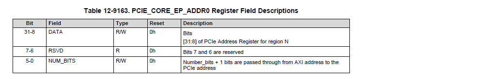
1. I cannot found the register description of PCIE_CORE_RP_ADDR0 (0x0D400000), the TRM only has  PCIE_CORE_EP_ADDR0 register description.

I referred J721E_DRA829/TDA4VM/AM752x_SR1.0_TRM. Can you tell me how to use PCIE_CORE_RP_ADDR0?

2.TRM tells the GIC-ITS translator address is 0x1000000 (COMPUTE_CLUSTER0_GIC_TRANSLATER 01000000h) not  base from 0x1800000, but when I use 0x1800000 or 0x10000000 as translator address base, both works. whether means 0x1000000 and 0x1800000 both OK?

  • Hi,

    I got the following feedback from the TRM team:

    1.

    The PCIE register content has been updated in the latest TRM revision A.

    Please refer to the J721E_DRA829_TDA4VM_AM752x_SR1.0_TRM vA.

     At address 0x0D400000 resides the PCIE_CORE_ATU_WRAPPER_OB_0_ADDR0 register which contains bits 31:8 of the PCIe address and the number of AXI address bits passed through for outbound region 0.

    The PCIE supports 32 outbound address translation regions.

    2.

    TI recommends to use only address 0x10000000 (GIC region 1) for GITS_TRANSLATER operations. Accessing GITS_TRANSLATER through address 0x01830000 (offset 30000 in GIC region 0) should not be used.

    hope this helps.

    regards,

    Stan

  • Hi Stan,

    Thanks for you quick reply.

    I have only J721E_DRA829_TDA4VM_AM752x_SR1.0_NDA_TRM_vInitial.pdf.

    You wrote:

    "At address 0x0D400000 resides the PCIE_CORE_ATU_WRAPPER_OB_0_ADDR0 register which contains bits 31:8 of the PCIe address and the number of AXI address bits passed through for outbound region 0."

    It seems to be the same with EP description not RC.

    Below is I copied from TI SDK linux. But I cannot found this information on TRM.

    /*
    * Address Translation Registers
    */
    #define CDNS_PCIE_AT_BASE 0x00400000

    /* Region r Outbound AXI to PCIe Address Translation Register 0 */
    #define CDNS_PCIE_AT_OB_REGION_PCI_ADDR0(r) \
    (CDNS_PCIE_AT_BASE + 0x0000 + ((r) & 0x1f) * 0x0020)
    #define CDNS_PCIE_AT_OB_REGION_PCI_ADDR0_NBITS_MASK GENMASK(5, 0)
    #define CDNS_PCIE_AT_OB_REGION_PCI_ADDR0_NBITS(nbits) \
    (((nbits) - 1) & CDNS_PCIE_AT_OB_REGION_PCI_ADDR0_NBITS_MASK)
    #define CDNS_PCIE_AT_OB_REGION_PCI_ADDR0_DEVFN_MASK GENMASK(19, 12)
    #define CDNS_PCIE_AT_OB_REGION_PCI_ADDR0_DEVFN(devfn) \
    (((devfn) << 12) & CDNS_PCIE_AT_OB_REGION_PCI_ADDR0_DEVFN_MASK)
    #define CDNS_PCIE_AT_OB_REGION_PCI_ADDR0_BUS_MASK GENMASK(27, 20)
    #define CDNS_PCIE_AT_OB_REGION_PCI_ADDR0_BUS(bus) \
    (((bus) << 20) & CDNS_PCIE_AT_OB_REGION_PCI_ADDR0_BUS_MASK)

    Can you help me check this in TI lastest TRM?

    Thank you!

  • Hi,

    That particular information in the SDK is currently missing from the TRM but will be added in a future revision.


    So, looking again at the register at address 0x0D400000 (that is, the ADDR0 register for Outbound Region 0):

    Bits [27-20] of field [31-8] DATA define the Bus Number.

    Bits [19-12] of field [31-8] DATA define the Function Number.

    These form the Completer ID information for a configuration TLP.

    When the Completer ID is conveyed through the Outbound AXI to PCIe Address Translation Registers, the [5-0] NUM_BITS field should be programmed to 6'd11.

  • Hi Stanislav,

    Thanks for your information above. 

    more question

    1.I see the register description of PCIE_CORE_LM_I_RC_BAR_CONFIG_REG Register (Offset = 00100300h)

    At bit20 (RCBARPIS) Width of IO Base and Limit registers in type1 config space.
    0=32 bits,
    1=64 bits

    Is this incorrect?

    or correct should be:

    0=16 bits,
    1=32 bits


    2. I see a known issue about PCIE RC

    2.1.6.4. Known issues & limitations

    Record IDSummaryWorkaround
    LCPD-16396 J721E: RC: Unsupported request in configuration completion packets results in an abort Workaround for Multifunction: Configure all the physical functions supported by the endpoint.

    How can I get the detail information about LCPD-16396? Is there workaround patch for linux?

    Thanks!

  • Hi Jun,

    1. we checked the specs and the correct is:

    0=32 bits,
    1=64 bits


    2. I will ping Linux experts to comment on this.

    Regards,

    Yordan

  • 1. we checked the specs and the correct is:

    0=32 bits,
    1=64 bits

    =>

    But I saw in linux  it define as below:

    /* Root Complex BAR Configuration Register */
    #define CDNS_PCIE_LM_RC_BAR_CFG (CDNS_PCIE_LM_BASE + 0x0300)
    #define CDNS_PCIE_LM_RC_BAR_CFG_BAR0_APERTURE_MASK GENMASK(5, 0)
    #define CDNS_PCIE_LM_RC_BAR_CFG_BAR0_APERTURE(a) \
    (((a) << 0) & CDNS_PCIE_LM_RC_BAR_CFG_BAR0_APERTURE_MASK)
    #define CDNS_PCIE_LM_RC_BAR_CFG_BAR0_CTRL_MASK GENMASK(8, 6)
    #define CDNS_PCIE_LM_RC_BAR_CFG_BAR0_CTRL(c) \
    (((c) << 6) & CDNS_PCIE_LM_RC_BAR_CFG_BAR0_CTRL_MASK)
    #define CDNS_PCIE_LM_RC_BAR_CFG_BAR1_APERTURE_MASK GENMASK(13, 9)
    #define CDNS_PCIE_LM_RC_BAR_CFG_BAR1_APERTURE(a) \
    (((a) << 9) & CDNS_PCIE_LM_RC_BAR_CFG_BAR1_APERTURE_MASK)
    #define CDNS_PCIE_LM_RC_BAR_CFG_BAR1_CTRL_MASK GENMASK(16, 14)
    #define CDNS_PCIE_LM_RC_BAR_CFG_BAR1_CTRL(c) \
    (((c) << 14) & CDNS_PCIE_LM_RC_BAR_CFG_BAR1_CTRL_MASK)
    #define CDNS_PCIE_LM_RC_BAR_CFG_PREFETCH_MEM_ENABLE BIT(17)
    #define CDNS_PCIE_LM_RC_BAR_CFG_PREFETCH_MEM_32BITS 0
    #define CDNS_PCIE_LM_RC_BAR_CFG_PREFETCH_MEM_64BITS BIT(18)
    #define CDNS_PCIE_LM_RC_BAR_CFG_IO_ENABLE BIT(19)
    #define CDNS_PCIE_LM_RC_BAR_CFG_IO_16BITS 0
    #define CDNS_PCIE_LM_RC_BAR_CFG_IO_32BITS BIT(20)
    #define CDNS_PCIE_LM_RC_BAR_CFG_CHECK_ENABLE BIT(31)

  • Hi 

    Any news about the linux patch of LCPD-16396?

  • HI

    LCPD-16396 should not impact Use case where you have a directly connected EP device to the RC.eg. PCIe NVMe card.

    It only impacts use case scenario, where we have devices connected behind an external PCIe switch or when the device supports multiple functions and additionally the function numbering is not contiguous leaving a hole

    Under such scenario, when the device enumeration is done, querying for an non-existent function will result in a UR response.

    There is no workaround for this